| Posted: Oct 19, 2017 |
Terahertz spectroscopy goes nano
(Nanowerk News) Brown University researchers have demonstrated a way to bring a powerful form of spectroscopy -- a technique used to study a wide variety of materials -- into the nano-world.
|
|
Laser terahertz emission microscopy (LTEM) is a burgeoning means of characterizing the performance of solar cells, integrated circuits and other systems and materials. Laser pulses illuminating a sample material cause the emission of terahertz radiation, which carries important information about the sample's electrical properties.
|
|
"This is a well-known tool for studying essentially any material that absorbs light, but it's never been possible to use it at the nanoscale," said Daniel Mittleman, a professor in Brown's School of Engineering and corresponding author of a paper describing the work. "Our work has improved the resolution of the technique so it can be used to characterize individual nanostructures."
|
|
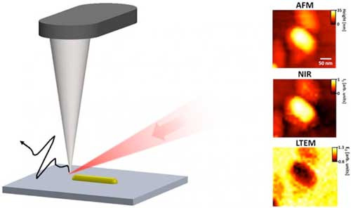
Typically, LTEM measurements are performed with resolution of a few tens of microns, but this new technique enables measurements down to a resolution of 20 nanometers, roughly 1,000 times the resolution previously possible using traditional LTEM techniques.
|
 |
| Researchers have improved the resolution of terahertz spectroscopy by 1,000 times, making the technique useful at the nanoscale. (Image: Mittleman Lab / Brown University)
|
|
The research, published in the journal ACS Photonics ("Nanoscale Laser Terahertz Emission Microscopy"), was led by Pernille Klarskov, a postdoctoral researcher in Mittleman's lab, with Hyewon Kim and Vicki Colvin from Brown's Department of Chemistry.
|
|
For their research, the team adapted for terahertz radiation a technique already used to improve the resolution of infrared microscopes. The technique uses a metal pin, tapered down to a sharpened tip only a few tens of nanometers across, that hovers just above a sample to be imaged. When the sample is illuminated, a tiny portion of the light is captured directly beneath the tip, which enables imaging resolution roughly equal to the size of the tip. By moving the tip around, it's possible to create ultra-high resolution images of an entire sample.
|
|
Klarskov was able to show that the same technique could be used to increase the resolution of terahertz emission as well. For their study, she and her colleagues were able to image an individual gold nanorod with 20-nanometer resolution using terahertz emission.
|
|
The researchers believe their new technique could be broadly useful in characterizing the electrical properties of materials in unprecedented detail.
|
|
"Terahertz emission has been used to study lots of different materials -- semiconductors, superconductors, wide-band-gap insulators, integrated circuits and others," Mittleman said. "Being able to do this down to the level of individual nanostructures is a big deal."
|
|
One example of a research area that could benefit from the technique, Mittleman says, is the characterization of perovskite solar cells, an emerging solar technology studied extensively by Mittleman's colleagues at Brown.
|
|
"One of the issues with perovskites is that they're made of multi-crystalline grains, and the grain boundaries are what limits the transport of charge across a cell," Mittleman said. "With the resolution we can achieve, we can map out each grain to see if different arrangements or orientations have an influence on charge mobility, which could help in optimizing the cells."
|
|
That's one example of where this could be useful, Mittleman said, but it's certainly not limited to that.
|
|
"This could have fairly broad applications," he noted.
|

