| Posted: Oct 24, 2017 |
Scientists invent a new mode of atomic force microscopy (AFM)
(Nanowerk News) Atomic Force Microscopy (AFM) is one of the most buoyant techniques in material characterization. This important boom lies in the versatility of this type of microscope: it is not only possible to see the materials, but also to study other properties that could not be measured such as their electrical, magnetic or thermal properties.
|
|
This versatility has made AFM a far-reaching technique for characterization of materials, which already assumes an industry by itself that reports $ 400 million in profits annually.
|
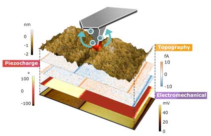 |
| 3D composition in which the tip that scans the surface along with the rest of the properties of the material is represented, such as the generation of charge (measured in current, femtoAmpere scale) as well as its electromechanical response. Image size is 30 by 15 micrometers.
|
|
Within this technique, there are different modes of measurement, depending on the property to be studied. For example, if you want to study if a material is electrically conductive, there is a technique called "Conductive Atomic Force Microscopy" (CAFM) for this purpose. In the paper, published in Nature Communications ("Piezo-generated charge mapping revealed through direct piezoelectric force microscopy"), a group of scientists from the CSIC, together with scientists from the CNRS, have implemented a new method of microscopy called Direct Piezoelectric Force Microscopy.
|
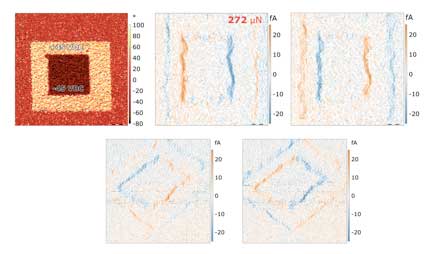 |
| Images of a ferroelectric material composed by Bismuth Ferrite in which a ferroelectric pattern has been recorded to the nanoscale with voltages of +45 VDC and -45 VDC, scale bar is 2.5 micrometers. Then, each analysis is performed with the new mode, DPFM, which provides the loads generated by piezoelectric effect.
|
|
"This technique allows us to measure the small currents that are generated by piezoelectric effect in a quantitative way and to the nanoscale," remarks Andrés Gómez. Piezoelectric materials, discovered in 1880 by the Curies, are capable of generating small electrical charges by being mechanically compressed.
|
|
Piezoelectric materials, on their own, make up a $1 bn industry, their characterization being one of the most important keys to their development.
|
|
"The technique allows to study the piezoelectricity with a microscope of atomic forces in the opposite direction to the habitual one. Until now, a voltage was applied to the tip of the AFM and it was seen how the material contracted or expanded as a function of that voltage. We measure it backwards, apply force, and measure the current that is generated," says Gómez.
|
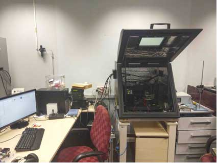 |
| Image of the microscope where the new mode of characterization of piezoelectric materials has been implemented.
|
|
This new AFM mode enhances this microscopy technique as a standard characterization technique available for material research specifically for the case of piezoelectricity and ferroelectricity.
|
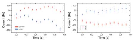 |
| Current (fA) recorded while performing a standard Approach and retract curve over a piezoelectric material from Morgan Advanced Materials, PZT5A1. The left frame corresponds to a up polarization state, while the right frame corresponds to the opposite polarization (the sample was flipped). Red curve is the approach process, when the force is increasing, while the blue curve corresponds to the retract process, where the tip is decreasing its force.
|

