| Posted: Nov 22, 2017 |
Shedding light on the behavior of electrical contacts in carbon semiconductor nanotubes
(Nanowerk News) A team of Skoltech scientists, in collaboration with researchers from the IBM Watson Research Center, have shed light on the behavior of electrical contacts in carbon semiconductor nanotubes – a revelation that could pave the way to next-generation electronics (Physical Review Letters, "Band Structure and Contact Resistance of Carbon Nanotubes Deformed by a Metal Contact").
|
|
Carbon is extremely tough and relatively light with unique electronic and optical properties. Since their discovery some 20 years ago, scientists have been actively investigating their myriad potential uses, as well as their unique properties. As an example, carbon nanotubes are known to conduct electricity significantly more efficiently than other materials, such as silicon and copper.
|
|
Silicon digital electronics have revolutionized our experience of the world. Silicon microprocessors are found in technologies ranging from mobile phones to jumbo jets. In the past, tech devices were made possible by a reduction in transistor size, but the possibilities of silicon have effectively reached their limit; thus, it is necessary to search for new opportunities to reduce costs and increase performance in electronic devices.
|
|
Toward this end, technology giants like IBM are actively investigating their potential to replace silicon in next-generation computers and other electronics. The primary challenge in this regard is contact resistance, which is attributable to the low resistance of nanotube channels.
|
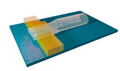 |
| Schematic of a carbon nanotube field-effect transistor contact.
|
|
“Transistor resistance includes both channel and contact resistance. The channel resistance of carbon nanotubes is better than that of silicon, but no one needs transistors made of nanotubes with a long channel, and when the tube size decreases to several tenths of a nanometer, the contact resistance begins to dominate,” said Skoltech Professor Vasili Perebeinos, the study’s lead author.
|
|
Semiconductor tubes are used to manufacture transistors. But metal is used for contacts. Metal exerts pressure on the tubes, which comes at the expense of surface tension. Previous research in the field revealed that this pressure is high enough to flatten the tubes.
|
|
“In our latest research, we, quite unexpectedly, predicted that semiconductor tubes flattened by a metal contact become metallic. In this case, the contact resistance increases, and does not subsequently decrease. This is due to the breaking of the axial symmetry of the deformed tubes under the metal contact,” Perebeinos said.
|
|
The Skoltech-led team’s research has helped elucidate the steps that can be taken to reduce contact resistance. They determined that for purposes of manufacturing transistors, it’s preferable to use tubes with relatively small diameters.
|
|
To put this into context, we can imagine a comparable situation in the macro world. Imagine a large pipe instead of a nanotube, and a hammer pounding against the pipe instead of metal exerting pressure. It immediately becomes clear why a diametric reduction would help; it would be easier to flatten a pipe with a large diameter than one with a smaller diameter.
|
|
It is also possible to use metals with a lower surface tension; the “hammer blow” in this case would be weaker and the nanotube would not be flatten.
|

