| Posted: Nov 30, 2017 |
Craters on graphene: Electrons impact(Nanowerk News) Imaging electrons can help scientists better understand exotic electronic states, such as electricity that travels through wires without loss. The team created images of superfast electrons trapped as they tunnel through energy barriers in graphene. They visualized this unusual tunneling for the first time (Nature Physics, "Imaging electrostatically confined Dirac fermions in graphene quantum dots"). |
| They did it by imaging the density of charge carriers in a circular junction in a graphene layer on top of insulating boron nitride. Charge carriers are excited electrons and their holes (positively charged spots where the electrons resided before becoming excited). |
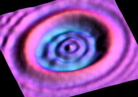 |
| Trapped electrons that follow the rules of relativistic quantum mechanics were directly imaged, validating theoretical predictions that these electrons traveling at near the speed of light can tunnel through energy barriers. The map shows the circular interference patterns of a graphene quantum dot, where the standing wave near the center of the dot arises from confined electronic states. This 300- by 300-nanometer map, representing a region that is a fraction of the size of the head of a pin, was obtained with a scanning tunneling microscope. The contrast corresponds to differences in conductance. (Image: Lawrence Berkeley National Laboratory) |
| With this new knowledge of electron physics, we better understand how energy moves through graphene. Controlling electrons’ behavior could open the door for new graphene-based devices. These devices could enable faster, higher performing computers and sensors. |
| Normally, electrons moving in a conductor are reflected by potential energy barriers. However, electrons moving in graphene travel at relativistic velocities (near the speed of light) and behave very differently. Theory predicts that some of these electrons will be unaffected by the potential barrier and tunnel directly through it. |
| In a particular type of tunneling called Klein tunneling, particles can burrow through potential barriers with perfect transmission. In pristine graphene, this allows high mobility electronic transport but hinders electrostatic confinement of charge carriers necessary for practical applications. |
| Scientists predicted that circular graphene junctions could trap electrons for short periods of time, resulting in the formation of graphene quantum dots. The researchers made these quantum dots by a novel scanning tunneling microscopy technique that manipulates the local defect charge within an insulating boron nitride substrate by electrostatic gating. Nanoscale graphene junctions were thus created, probed, and imaged. |
| Images validated theoretical predictions and demonstrated that graphene charge carriers could be electrostatically confined by artificial potentials. This work provides a new experimental platform for understanding and controlling the spatial behavior of charge carriers in graphene. |
| Source: U.S. Department of Energy (DOE), Office of Science |

