| Posted: Dec 01, 2017 |
Wafer to chip: X-ray imaging for reduced defect rate(Nanowerk News) Using non-destructive imaging methods, a team of scientists at KIT obtains three-dimensional insights into the interior of crystals. They determine important data about line-shaped defects that largely influence the deformation behavior of crystals. These so-called dislocations impede the production of computer chips. As reported in the Physical Review Letters ("Correlated Three-Dimensional Imaging of Dislocations: Insights into the Onset of Thermal Slip in Semiconductor Wafers"), the scientists combine two X-ray methods with a special type of light microscopy. |
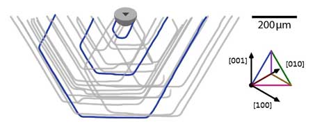 |
| When processing semiconductor wafers, small surface defects may lead to large defects inside and to steps on large surface areas. (Image: D. Hänschke/KIT) |
| Even a few dislocations in silicon wafers can lead to defective computer chips and, hence, to undesired production rejects. “It is therefore important to understand how a minor mechanical surface defect propagates into the depth of the crystal under typical process impacts, such as heat,” says Dr. Daniel Hänschke, physicist of KIT’s Institute for Photon Science and Synchrotron Radiation. |
| His team has succeeded in precisely measuring dislocations and studying their interactions with each other and with external impacts. The scientists analyzed how a single surface defect spreads into an armada of hexagonal defect lines, while completely undamaged areas may remain in the center of such a three-dimensional network. “The resulting collective movement can raise or lower large surface areas on the opposite side of the wafer and cause the formation of steps, which may adversely affect the fabrication and function of microstructures,” Hänschke points out. |
| Combined with mathematical model calculations, the results allow to better understand the underlying physical principles. “Models used so far are mainly based on data measured by electron microscopy in very small crystal samples,” Dr. Elias Hamann, another member of the team, explains. “Our method can also be applied to study large, flat crystals, such as commercially available wafers,” he adds. “This is the only way to determine detailed relationships between the initial, minute original damage and the resulting extensive crystal deformations that may cause major problems far away from the onset of the defect.” |
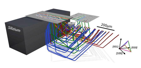 |
| When processing semiconductor wafers, small surface defects may lead to large defects inside and to steps on large surface areas. (Image: D. Hänschke/KIT) (Silizium = Silicon) |
| The new measurement method combines X-ray techniques at the KARA synchrotron of KIT and the ESRF European synchrotron in Grenoble with so-called CDIC light microscopy. The findings obtained will help improve existing models for the prognosis of defect formation and defect propagation and, hence, provide indications of how the fabrication process of computer chips can be optimized. The number of transistors arranged on a square centimeter of a wafer surface already reaches several billions, with increasing tendency. Even smallest defects on and in the crystal may cause thousands of these small circuits to fail and the corresponding chips to be unusable. Industry is highly interested in further minimizing the defect rate in the future. |
| Source: Karlsruhe Institute of Technology |

