| Posted: Dec 12, 2017 |
Scientists suggested a new technology for creating magnet micro-structures
(Nanowerk News) A team of scientists from Krasnoyarsk Scientific Center (Siberian Department of Russian Academy of Sciences) and Siberian Federal University synthesized thin crystal ferromagnetic films and developed a technology for their shaping. Processed films can be used in electronic and spintronic chips. The results of the study were published in Thin Solid Films.
|
|
The team created films that are hundreds to dozens nanometers thick. The developed films are formed of iron silicides synthesized on a silicon substrate. Iron silicides are compounds of iron and silicon that usually have ferromagnetic properties when subject to certain temperatures. There are also non-magnetic iron silicides with unique optic characteristics that may be put to practical use.
|
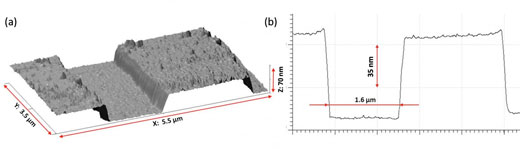 |
| This is the configuration of a thin crystal film. (Image: Anton Tarasov)
|
|
Films like this are used as active parts in optic and photonic devices, as well as in integral electronic and spintronic chips. Thin ferromagnetic films open a lot of prospects for spintronics (an area of science that provides for the creation of information storage and processing devices). Devices like this consume less electrical energy and have higher operating speed compared to traditional electronic ones.
|
|
However, to develop such devices scientists need films to be specifically shaped. It means that a template has to be applied to synthesized films, and they have to be cut according to it. To do so, scientists use etching. It can be either wet (chemical) or dry (plasma, reactive-ion, or just ion). In the course of wet etching a film is placed in liquid - an etching agent that dissolves the rest of it. Before that scientists cover the films with "masks" using photolitography to set out required configuration. Such a mask protects the desired part of the film from solving. In dry etching the same result is achieved using a gas that destroys the material physically or chemically.
|
|
"We've broadened the application of this approach, extended it to new iron-silicon alloys, and showed that it works. We've also determined the speed of etching and developed a micro-device. The same methods may be used for the production of different structures in electronics, photonics, and other applications," said Anton Tarasov, a co-author of the article, candidate of physical and mathematical sciences, a scientific associate of Kirensky Institute of Physics (FRC KSC of SD RAS), and senior tutor at Siberian Federal University.
|
|
Scientists point out that a big advantage of the new films is not only their electronic and magnetic properties, but compatibility with the most popular technological semiconductors. It means, these films may be grown on bases made of silicon, germanium, and gallium arsenide. This will help the team obtain high-quality thin films with specific shapes and geometry in a simpler and more affordable way. Moreover, the obtained results increase the selection of materials that scientists may use to develop different devices.
|
|
"Using this technology, one can create spintronic or photonic devices, because iron silicides have properties applicable in these areas of science. Right now we are growing new films and studying the effects that depend on their topology," concluded the scientist.
|
|
The team worked in collaboration with scientists from Siberian State Aerospace University and Lomonosov Moscow State University. The research was supported with grants from Russian Foundation for Basic Research and Krasnoyarsk Regional Science Foundation, as well as with the grant of the President of the Russian Federation for the support of leading scientific establishments.
|

