| Posted: Dec 13, 2017 |
Light perfects interfaces(Nanowerk News) Improving electronic devices demands materials perform multiple functions. To create such materials, scientists often need to grow semiconducting films on dissimilar materials. Attempts to grow such films can result in a highly defective interface and unusable devices. |
| Scientists deposited atoms in precise layers by directing beams of elements at the surface. During growth, the light tuned the mixture of chemical bonds at the interface. Using this approach, researchers grew a nearly perfect zinc selenide film on a gallium arsenide surface even though their chemistries are dissimilar (Scientific Reports, "Tailoring heterovalent interface formation with light"). |
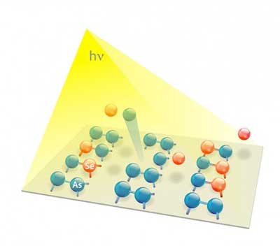 |
| High-quality interfaces and functionality may be possible in materials for electronic devices if the desired semiconductor is exposed to ultraviolet light during growth. Beams of zinc selenide (ZnSe) are deposited to grow films on gallium arsenide. Light exposure enhances desorption of arsenic atoms (blue) from a gallium arsenide surface, creating openings for selenium atoms (red) to bond with underlying gallium atoms. (Image: National Renewable Energy Laboratory) |
| There is a growing need for new, tailored materials that handle light and electricity. This research produced high-quality films suitable for these applications. At the same time, this work furthered our understanding of how shining light during semiconductor growth affects the formation of interfaces and the quality of the deposited layers. |
| The revolution of the microelectronics technology was made possible by the growth of high-quality semiconductor materials. In a technique called molecular beam epitaxy, atoms are deposited one layer at a time to grow semiconducting films. |
| A historical challenge has been to grow one semiconductor on a different semiconductor because the chemistries are dissimilar. The interface between dissimilar materials often contains defects that degrade the properties. |
| One example is the growth of zinc selenide (ZnSe) on gallium arsenide (GaAs). Defects form at their interface as a consequence of the differences in the number of electrons each element provides for bonding. |
| Recently, ultraviolet illumination was used to controllably tune the types of bonds that are formed when a layer of ZnSe was grown at low temperature on a layer of GaAs. Modification of the bonds at the interface minimized the formation of defects. |
| In this study, researchers used an ultraviolet lamp to first illuminate an uncoated GaAs substrate, which was observed to partially desorb excess surface arsenic atoms. The team continued the ultraviolet illumination during the deposition of ZnSe. An analysis of the resulting structure showed a sharp ZnSe-GaAs interface with minimal defects. |
| These results show that low-temperature growth accompanied by moderate ultraviolet photon irradiation can be used to tailor the structure of the interface and improve the optical quality of the ZnSe on GaAs layers. |
| Source: Department of Energy, Office of Science |

