| Posted: Dec 14, 2017 |
Nanoparticle staircase: Atomic blasting creates new devices to measure nanoparticles
(Nanowerk News) Like sandblasting at the nanometer scale, focused beams of ions ablate hard materials to form intricate three-dimensional patterns. The beams can create tiny features in the lateral dimensions--length and width, but to create the next generation of nanometer-scale devices, the energetic ions must precisely control the features in the vertical dimension--depth. Now, researchers at the National Institute of Standards and Technology (NIST) have demonstrated that a standard ion-beam technique can be fine-tuned to make structures with depths controlled to within the diameter of a single silicon atom.
|
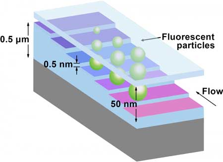 |
| A nanofluidic staircase machined with subnanometer precision by a focused ion beam separates nanoparticles by size. The device is also a reference material to accurately measure nanoparticle size and compare it to optical brightness, which could aid in the quality control of consumer products. (Image: NIST)
|
|
Taking advantage of that newly demonstrated precision, the NIST team used this standard machining technique to fabricate devices that allow precise measurement of the size of nanoparticles in a liquid. The nanofluidic devices, which have the potential for mass production, could become a new laboratory standard for determining nanoparticle size. Such measurements could expedite quality control in industrial applications of nanoparticles.
|
|
"We have tested and advanced what is possible to make and measure below one nanometer," said NIST researcher Samuel Stavis. He and his colleagues from NIST and the Maryland NanoCenter at the University of Maryland in College Park reported their findings in a recent issue of Lab on a Chip ("Subnanometer structure and function from ion beams through complex fluidics to fluorescent particles").
|
|
Although engineers have for years used ion beams to fix defects in integrated circuits and machine tiny parts in optical and mechanical systems, those applications did not require the depth control the team has now reported.
|
|
To realize the full potential of the process, the team explored several ways of using a focused beam of gallium ions to mill the surfaces of silicon, silicon nitride and silicon dioxide--materials that are common for the fabrication of nanoscale devices used in electronics, optics and mechanics. The researchers used an atomic force microscope, which features a sensitive probe to measure the depth of the topography formed by the ion beam. Careful measurements were important to testing the limits of the ion-beam technique. The facilities at NIST enabled the team to undertake both tasks--precision fabrication and precision measurement.
|
|
The team applied the new capability to improve the measurement of the size of nanoparticles. Using a gallium ion beam, the researchers machined staircase patterns in silicon dioxide and then enclosed them to control the flow of fluid at the nanoscale. In some devices, the researchers machined a staircase with a step size of 1.1 nanometers; they machined others with a step size of 0.6 nanometers--just a few atoms in depth.
|
|
The steps of the staircase pattern precisely separated nanoparticles immersed in water according to their size. Nanoparticles flowed in to the deepest step at the bottom of the staircase, but only the smaller ones could ascend towards the shallowest step at the top; larger nanoparticles could not fit through and remain trapped at the bottom set of steps. Fluorescent dye within the nanoparticles enabled the team to record their location with an optical microscope and match that location to the known depth of the staircase.
|
|
Comparing the nanoparticle sizes indicated by this method with the sizes measured using electron microscopy revealed a match that was accurate to within one nanometer. This good agreement of the different measurements suggests that the devices can serve not only as a particle separator but as a reference material for measuring the sizes of nanoparticles.
|
|
Manufacturers who routinely perform quality control on nanoparticles--determining not only their average size, but how many of the nanoparticles are slightly smaller or larger than average from batch to batch--could benefit from the new technique. The newly fabricated devices, in combination with an inexpensive optical microscope to pinpoint the locations of nanoparticles, offer a potentially faster and more economical route than other measurement techniques, Stavis noted. The team is now investigating how the devices could serve as master molds for the mass production of inexpensive replicas.
|
|
Because the nanoparticles were measured with an optical microscope, the NIST team could also explore the relationship between the size of nanoparticles and another key property--their brightness. Clarifying that relationship is important for understanding the properties of such nanoparticles as quantum dots for color displays, gold nanoparticles for biomedical sensors, and other nanoparticles for drug delivery.
|
|
The team detailed their process so that researchers at NIST can readily take advantage of and adapt the process for their own work. Several customers of NIST's nanotechnology user facility, the Center for Nanoscale Science and Technology, where the work was conducted, have expressed interest in adapting the technology for measuring both the size and brightness of nanoparticles in these consumer products.
|

