| Posted: Dec 22, 2017 |
Escaping silicon(Nanowerk News) A systematic study of a simple and general structure for on-chip semiconductor lasers by A*STAR researchers sets the scene for much broader application of integrated semiconductor lasers beyond conventional silicon-based systems (Applied Optics, "Comparison of III-V/Si on-chip lasers with etched facet reflectors"). |
| The ability to use, manipulate and sense light is applicable to many technologies, from data interconnection and fiber optics to optical sensors and optical storage systems. Tiny lasers are routinely integrated into microchips for these ‘optoelectronics’ applications using a well-understood silicon-based laser structure, but alternative and potentially simpler structures in non-silicon systems have yet to be explored in detail. |
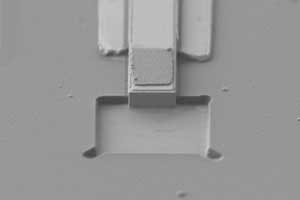 |
| An etched facet semiconductor laser with an air gap reflector. (© Optical Society of America) |
| One such non-silicon-based application is a new type of data storage system called heat-assisted magnetic recording (HAMR), which researchers at the A*STAR Data Storage Institute have been working on as a next-generation data storage technology. HAMR uses integrated lasers for fast and precise micro-spot heating of a magnetic medium, but requires the laser to be formed on aluminum-titanium-carbide (AlTiC) rather than silicon. This presented Chee-Wei Lee and his colleagues with a significant problem, since the silicon substrate plays in integral role in producing the laser light. |
| “We needed to develop a generic integration scheme that would allow us to fabricate laser devices on different substrates, not just silicon,” says Lee. “For this, a facet reflector structure is very useful, but low facet reflectivity is a problem, and using different reflectors usually means a more complicated fabrication process and greater chance of device failure.” |
| The lasers used in such applications turn electrical current into a light emission. They do this by taking light produced by a stack of ultrathin layers of a light-emitting semiconductor (in this case aluminum-gallium-indium-arsenide), and multiplying light at the target wavelength using a resonant cavity formed between two reflectors. |
| By designing a faceted laser structure considering process integration, Lee and his team developed a fabrication scheme that can accommodate different types of reflectors without additional processing steps. The team then used this fabrication scheme to test facet reflectors made by depositing a thin gold film, by chemical modification of the surface, or by etching an air gap (see image). |
| Studies of the different laser structures fabricated in the A*STAR laboratory and supporting simulations revealed that a thin gold layer, less than 100 nm thick, afforded the best performance in terms of facet reflectivity, minimum lasing current, emission efficiency and output power. |
| “We expect our results to serve as benchmark for research and development on etched facet lasers with different reflectors,” says Lee. |
| Source: A*STAR |

