| Posted: Jan 03, 2018 |
Carbon nanotubes devices may have a limit to how 'nano' they can be
(Nanowerk News) Carbon nanotubes bound for electronics not only need to be as clean as possible to maximize their utility in next-generation nanoscale devices, but contact effects may limit how small a nano device can be, according to researchers at the Energy Safety Research Institute (ESRI) at Swansea University in collaboration with researchers at Rice University.
|
|
Carbon nanotubes devices may have a limit to how “nano” they can beESRI Director Andrew Barron, also a professor at Rice University in the USA, and his team have figured out how to get nanotubes clean enough to obtain reproducible electronic measurements and in the process not only explained why the electrical properties of nanotubes have historically been so difficult to measure consistently, but have shown that there may be a limit to how “nano” future electronic devices can be using carbon nanotubes.
|
|
Like any normal wire, semiconducting nanotubes are progressively more resistant to current along their length. But conductivity measurements of nanotubes over the years have been anything but consistent. The ESRI team wanted to know why.
|
|
“We are interested in the creation of nanotube based conductors, and while people have been able to make wires their conduction has not met expectations. We were interested in determining the basic sconce behind the variability observed by other researchers.”
|
|
They discovered that hard-to-remove contaminants -- leftover iron catalyst, carbon and water -- could easily skew the results of conductivity tests. Burning them away, Barron said, creates new possibilities for carbon nanotubes in nanoscale electronics.
|
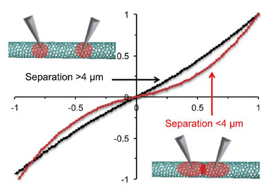 |
| Two-point probe and Raman spectroscopy have been used to investigate the effects of vacuum annealing and argon bombardment, on the conduction characteristics of MWCNTs. Surface contamination has a large effect on the two-point probe conductivity measurements resulting in inconsistent and non-reproducible contacts as well as enhancing the electric field under the contacts resulting from overlapping depletion regions when probe separations are small (<4 µm) causing very high resistances. (© ACS)
|
|
The new study appears in the American Chemical Society journal Nano Letters ("Spatial and contamination dependent electrical properties of carbon nanotubes").
|
|
The researchers first made multiwalled carbon nanotubes between 40 and 200 nanometers in diameter and up to 30 microns long. They then either heated the nanotubes in a vacuum or bombarded them with argon ions to clean their surfaces.
|
|
They tested individual nanotubes the same way one would test any electrical conductor: By touching them with two probes to see how much current passes through the material from one tip to the other. In this case, their tungsten probes were attached to a scanning tunneling microscope.
|
|
In clean nanotubes, resistance got progressively stronger as the distance increased, as it should. But the results were skewed when the probes encountered surface contaminants, which increased the electric field strength at the tip. And when measurements were taken within 4 microns of each other, regions of depleted conductivity caused by contaminants overlapped, further scrambling the results.
|
|
"We think this is why there's such inconsistency in the literature," Barron said.
|
|
“If nanotubes are to be the next generation lightweight conductor, then consistent results, batch-to-batch, and sample-to-sample, is needed for devices such as motors and generators as well as power systems.”
|
|
Annealing the nanotubes in a vacuum above 200 degrees Celsius (392 degrees Fahrenheit) reduced surface contamination, but not enough to eliminate inconsistent results, they found. Argon ion bombardment also cleaned the tubes, but led to an increase in defects that degrade conductivity.
|
|
Ultimately they discovered vacuum annealing nanotubes at 500 degrees Celsius (932 Fahrenheit) reduced contamination enough to accurately measure resistance, they reported.
|
|
To now, Barron said, engineers who use nanotube fibers or films in devices modify the material through doping or other means to get the conductive properties they require. But if the source nanotubes are sufficiently decontaminated, they should be able to get the right conductivity by simply putting their contacts in the right spot.
|
|
“A key result of our work was that if contacts on a nanotube are less than 1 micron apart, the electronic properties of the nanotube changes from conductor to semiconductor, due to the presence of overlapping depletion zones” said Barron, “this has a potential limiting factor on the size of nanotube based electronic devices – this would limit the application of Moore’s law to nanotube devices.”
|

