| Posted: Feb 05, 2018 |
Taking solar energy to the edge
(Nanowerk News) At the Center for Integrated Nanotechnology (CINT), researchers discovered an efficient way to make combined solar panels and light-emitting devices. Rather than using blocks of hybrid perovskite materials, they layered several thin sheets on top of each other (Science, "Extremely efficient internal exciton dissociation through edge states in layered 2D perovskites" and Science, "Powering up perovskite photoresponse").
|
|
In this new layered pattern, they discovered important “layer-edge states.” In these states, energy is highly conserved. When excited by light or other sources, the material produces energy that doesn’t instantly dissipate and can be used to charge batteries or do other work. That is, it creates long-lived, free charge carriers that can be harvested and manipulated.
|
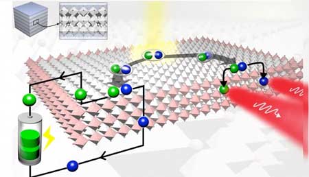 |
| An artistic rendering shows the dissociation of electron-hole pairs (excitons) to free carriers at crystal edges resulting in efficient solar energy (>12 percent) and light emission (>30 percent). Dissociated carriers captured and located at the edges have lower energy and last longer. (Image: Jean-Christophe Blancon, Los Alamos National Laboratory)
|
|
Compared to blocks of material, layered sheets of perovskites offer a host of benefits. The sheets are more chemically stable, more environmentally friendly, and more tunable to fit the needs of new applications or experiments. Discovery of edge states opens new avenues for designing and fabricating efficient electronic devices which collect and emit light. These devices include low-cost solar cells, LEDs, laser diodes, and detectors.
|
|
Hybrid perovskites are a new class of low-cost materials that can capture and emit light. This material can be synthesized in several forms: bulk 3-D structures, 2-D crystal sheets, and 1-D rods. In particular, layered compounds can be created by stacking 2-D crystal sheets with thin organic layers in between.
|
|
Compared to bulk 3-D variations, these sheets of perovskites are intrinsically stable and widely tunable. Therefore, these thin sheets may have broad applications in a variety of technologies.
|
|
In this study, scientists from CINT as well as international collaborators describe a strategy to layer sheets of 2-D perovskites to drastically enhance the material’s optoelectronic properties. They found that in materials with three or more layers, charged particles (electrons and holes) become trapped at low-energy states near the edge of the crystal layers.
|
|
These carriers exhibit a 5-fold increase in their lifetime and do not lose energy to heat, resulting in tremendous improvements in efficiency for light-capturing devices.
|
|
On the flip side, devices that emit light are also tremendously more effective because trapped carriers can recombine very efficiently.
|
|
These results address a long-standing problem not just for the perovskite family but also for a large group of materials. Often, the edges and surface states of materials can degrade the optoelectronic properties.
|
|
Now, the structure of these materials can be chemically designed and engineered to achieve efficient flow of charge and energy leading to high-efficiency optoelectronic devices.
|

