| Posted: Feb 21, 2018 |
Spatial structure of bound hole states in black phosphorous(Nanowerk News) NUS chemists have discovered that the bound states of “holes” (the absence of an electron which leads to a net positive charge) in black phosphorus changes from an extended ellipse into a dumbbell shape when it is electrically excited, providing new insights for its use in next generation electronic devices (Nano Letters, "Resolving the spatial structures of bound hole states in black phosphorus"). |
| Phosphorus, a highly reactive element, can exist in a stable crystalline form known as black phosphorus (BP). BP is emerging as a potential two-dimensional (2D) material for the development of a new generation of electronic devices with faster transistors than those of today. This is due to its ability to have a tunable direct bandgap (for acting as a switch), high carrier mobility (for carrying charges at high speed) and outstanding in-plane anisotropic properties (for controlling conducting properties along a specific crystal orientation). |
| As the native defects and impurities introduced during the synthesis and processing of BP affect its material properties and device characteristics, it is important to have a better understanding of these effects at the atomic level, so as to develop devices with better performance. |
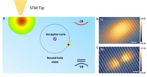 |
| (a) Illustration of the STM technique for probing bound hole states in BP. (b) Elliptical shape observed for the ground bound hole states (1s-like). (c) Dumbbell shape observed for the excited bound hole state (2px). Scale bar is 1 nm. |
| A team led by Prof LU Jiong from the Department of Chemistry, NUS has discovered that when BP goes from a non-excited ground state to an excited state, the spatial shape of its bound hole states evolves from an extended elliptical shape to a dumbbell shape. A bound state refers to the tendency of a particle to remain localised in a specific region when subjected to a potential field. |
| In BP, each hole interacts and orbits around the negatively charged core, forming bound hole states. This is analogous to the Bohr model for the hydrogen atom, in which the single electron encircles the atomic nucleus. The team made this discovery by using low temperature scanning tunnelling microscopy (STM), an atomic-resolution imaging technique, and operated it at 4.5 kelvin to probe the material surface. At such low temperature, the STM tip can be positioned over individual defects with an ultralow drift that is required for obtaining stable measurements. |
| Their findings provide a generic picture of the spatial structure and electronic properties of bound states near shallow dopants (which require little energy to produce free carriers) in BP. |
| Prof Lu said, “The unexcited bound hole state (1s) exhibits an anisotropic elliptical shape, in sharp contrast to the symmetrical 1s orbital shape of the hydrogen atom. The spatial shape is a result of the bound hole states being strongly extended along one crystal orientation while being compressed along another crystal orientation. Our study directly captures the anisotropic behaviours of individual hole carriers in BP, offering unprecedented atomic insights into high-mobility transport anisotropy of BP transistors”. |
| “We also demonstrated that the charge state of individual acceptors can be reversibly switched using the STM tip. The ability to manipulate the charge states of individual dopants may allow the realisation of a charge-based qubit and further development of quantum devices,” added Prof Lu. |
| Source: National University of Singapore |

