| Posted: Feb 22, 2018 |
Faster data transfer through plasmons
(Nanowerk News) Photonic and electronic devices could soon be successfully integrated thanks to new transducers developed by a team of Singaporean researchers that can generate, manipulate and read small packets of energy called surface plasmon polaritons (SPPs).
|
|
Photonic devices, which use light rather than electric charges to carry information, can operate thousands of times faster than conventional electronics, although they tend to be large and difficult to integrate with microchips.
|
|
The team of researchers led by Hong-Son Chu at the A*STAR Institute of High Performance Computing and Christian Nijhuis at the National University of Singapore believe that SPPs, electromagnetic surface waves that exist at the interface of two materials, could be used to seamlessly link photonic devices and electronics (Nature Photonics, "Highly efficient on-chip direct electronic-plasmonic transducers").
|
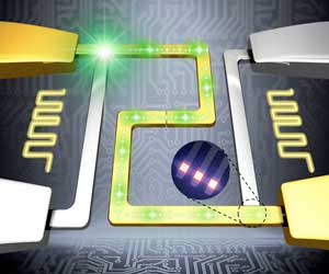 |
| This illustration shows two tunnel junctions coupled together by a plasmonic waveguide in the center. When a voltage is applied to the source junction, tunneling electrons excite surface plasmons, which propagate along the plasmonic waveguide and modulate the tunneling current at the detector junction. Inset: A light emission image of tunnel junctions, showing plasmons scattering from the end of the plasmonic waveguide. (Image: Du Wei, National University of Singapore)
|
|
“SPPs essentially contain light confined to dimensions smaller than its wavelength, and they function like photonic elements, carrying information at high speeds,” says Chu. “However, the SPPs offer the best of both worlds because they have the operational speed of optical elements as well as a small size suitable for nano-electronics applications. We have developed the first on-chip electronic-plasmonic transducers that operate at optical frequencies, and we achieved an electron-to-SPP conversion efficiency of more than 10 per cent.”
|
|
Most existing plasmonic devices require light sources such as LEDs to generate SPPs. This indirect method is quite slow. Chu and co-workers realized it would be much faster to produce SPPs by direct electrical means, so they designed transducers comprising aluminum and gold electrodes, separated by a two nanometer-thick layer of aluminum oxide that acts as an insulating ‘quantum tunneling’ barrier. Electrons that make the quantum leap across this gap will either generate or detect SPPs.
|
|
By joining two transducers with a plasmonic waveguide, so that one acted as a source and another as detector (see image), the researchers observed about 1 in 7 of the tunneling electrons coupling to a SPP. Although the reasons for this high tunneling rate are uncertain, Chu and co-workers suggest that SPPs at the junctions might induce an oscillating electric field, which changes the effective size of the tunneling gap and therefore the number of electrons that can cross the gap and interact with SPPs.
|
|
“By doing away with the need for light sources and detectors, devices based on this mechanism would be intrinsically fast,” says Chu. “Our work has attracted interest from research communities and industries, with potential applications in three-dimensional integrated circuits and high bandwidth memory devices. For example, there is a need for small, high-speed interconnectors to improve processing speeds.”
|

