| Posted: Mar 09, 2018 |
A bright idea for on-demand nanopatterns(Nanowerk News) An A*STAR team has assembled zinc sulfide (ZnS) quantum dots into nanoscale grids and arrays of lens-like disks by performing electron-beam lithography on a multipurpose thin film (ACS Nano, "Direct patterning of zinc sulfide on a sub-10 nanometer scale via electron beam lithography"). The photoluminescent properties of these patterns could make them useful components in applications such as biosensors and solar cells. |
| While individual ZnS nanoparticles have intriguing optical properties, due to the effects of quantum coupling, their light-emitting capabilities become more potent when positioned into ordered assemblies. Instead of conventional bottom-up approaches that use wet chemicals to generate nanoparticle ensembles on silicon chips, many researchers now approach this problem from the top down, using nanoscale lithography to strip away unwanted material and write quantum dots directly on to surfaces. |
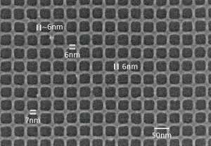 |
| Light-emitting ZnS nanostructures can be patterned into nearly any shape, including grids as above, using a multipurpose photoresist. (© ACS) |
| Carving shapes into semiconductor surfaces smaller than 10 nanometers is a particular expertise of M. S. M. Saifullah from the A*STAR Institute of Materials Research and Engineering, and colleagues. They direct high-powered electron beams on to special thin films called ‘resists’. Areas of the resist exposed to the focused beams undergo chemical changes that enable tiny features to stay in place while the surrounding film is washed away by solvents. |
| In most electron-beam lithography techniques, the patterned resist is transferred to another substrate and a chemical etching step generates the final nanoscale shapes. Saifullah and the team, however, had a different strategy. “We developed a resist that can decompose and form a metal sulfide right under the electron beam,” he notes. “This was a challenge because most resists don’t have such functionalities.” |
| The team found a compound called zinc butylxanthate that could meet their needs. In this molecule, zinc and sulfur atoms are connected to long-chain organic groups that potentially can be detached using the energy from an electron beam. Experiments with the new resist proved the efficiency of this conversion process: by gradually increasing the electron beam exposure, the starting film was transformed into ZnS nanocrystals with a conversion rate of almost 100 per cent |
| The A*STAR-led researchers exploited the properties of the zinc butylxanthate resist to produce lines of ZnS nanocrystals with diameters as thin as 6 nanometers. Then, after characterizing the structures with electron microscopy, they made another serendipitous discovery — the nanopatterns emitted bright photoluminescent light when exposed to ultraviolet radiation. Defect states on the nanocrystal surfaces were pinpointed as the cause of the new optical behavior. |
| “The nice thing about photoluminescent ZnS nanocrystals is they can be arranged into practically any shape,” says Saifullah. “In the future, we would like to combine these nanostructures with plasmonics.” |
| Source: A*STAR |

