| Posted: Mar 16, 2018 |
A better angle on microscopic devices
(Nanowerk News) Making increasingly smaller microelectromechanical systems (MEMS) has proved very challenging, limiting their anticipated potential. Now, researchers at A*STAR have developed a versatile and cost-effective technique for making devices with much greater precision and reliability for use in biotechnology and medical applications (Journal of Microelectromechanical Systems, "MEMS industry-worth etching to fabricate tapered structures in SiO2").
|
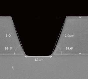 |
| Tapered contact opening fabricated by new two-step plasma etching process. (© IEEE)
|
|
MEMS are used in applications ranging from airbag systems and display screens, to inkjet cartridges. They are tiny devices that combine mechanical and electrical components. Current manufacturing technologies, however, are expensive and lack the precision for making devices with micron and sub-micron scale features.
|
|
This led Vladimir Bliznetsov and colleagues from the A*STAR Institute of Microelectronics to develop a versatile and low-cost method for fabricating MEMS at dimensions not previously possible, edging closer to the mass production of smaller and more reliable devices for a range of new applications.
|
|
“MEMS are following the general trend of miniaturization in electronics, with devices that are reducing in size from the tens of microns to one micron or less,” says Bliznetsov. “But the techniques used to manufacture top metal contacts to devices with such microscopic dimensions are costly and unreliable.”
|
|
Current methods for creating channels, called vias, with tapered sidewalls in MEMS at scales of five microns or less, are not dependable. The etching method, with sidewall polymerization, is not suitable as the width at the bottom of the vias shrink considerably. Another method, involving the transfer of a photoresist profile into an etched layer, limits the maximal depth of vias due to excessive loss of the photoresist mask resulting in unacceptably rough sidewalls.
|
|
To overcome these restrictions, the researchers developed a two-step plasma etching process. This combines firstly photoresist tapering, which modifies the photoresist from a vertical to a tapered profile, and then an oxide etching with sidewall polymerization with better selectivity to photoresist. This produces vias with minimal dimensions down to 1.5 microns, and smooth sidewalls with angles of around 70 degrees.
|
|
“We combined two effects which are usually harmful during the etching process — accelerated corner sputtering and sidewall polymerization,” explains Bliznetsov.
|
|
Combining these processes into a two-step method achieves greater control over the etching process and produces micron-sized vias with smooth, tapered walls. And by minimizing the sidewall angle of the vias, it is possible to fabricate devices that can be better protected and have more reliable metal contacts, greatly improving their performance.
|
|
“Precise control of sidewall angle has use in many applications, and we are now planning to fabricate functional magnetic memory cells, which require pillars of magnetic material with sidewalls having a specific angle,” says Bliznetsov.
|

