| Posted: Mar 16, 2018 |
Unexpected effect could lead to lower-power memory, computing devices
(Nanowerk News) An unexpected phenomenon known as zero field switching (ZFS) could lead to smaller, lower-power memory and computing devices than presently possible. The image shows a layering of platinum (Pt), tungsten (W), and a cobalt-iron-boron magnet (CoFeB) sandwiched at the ends by gold (Au) electrodes on a silicon (Si) surface. The gray arrows depict the overall direction of electric current injected into the structure at the back of the gold (Au) contact and coming out the front gold contact pad.
|
|
The CoFeB layer is a nanometer-thick magnet that stores a bit of data. A "1" corresponds to the CoFeB magnetization pointing up (up arrow), and a "0" represents the magnetization pointing down (down arrow). The "0" or "1" can be read both electrically and optically, as the magnetization changes the reflectivity of light shining on the material through another phenomenon known as the magneto-optical Kerr effect (MOKE).
|
|
In the device, electric current can flip the data state between 0 and 1. Previous devices of this type have also required a magnetic field or other more complex measures to change the material's magnetization. Those earlier devices are not very useful for building stable, non-volatile memory devices.
|
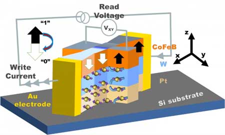 |
| This is an illustration of an unexpected phenomenon known as zero field switching (ZFS) that could lead to smaller, lower-power memory and computing devices than presently possible. The image shows a layering of platinum (Pt), tungsten (W), and a cobalt-iron-boron magnet (CoFeB) sandwiched at the ends by gold (Au) electrodes on a silicon (Si) surface. The gray arrows depict the overall direction of electric current injected into the structure at the back of the gold (Au) contact and coming out the front gold contact pad. The CoFeB layer is a nanometer-thick magnet that stores a bit of data. A "1" corresponds to the CoFeB magnetization pointing up (up arrow), and a "0" represents the magnetization pointing down (down arrow). (Image: Gopman/NIST)
|
|
A breakthrough occurred in a research collaboration between The Johns Hopkins University and NIST. The team discovered that they could flip the CoFeB magnetization in a stable fashion between the 0 and 1 states by sending only electric current through the Pt and W metal layers adjacent to the CoFeB nanomagnet. They did not need a magnetic field. This ZFS (zero-field switching) effect was a surprise and had not been theoretically predicted.
|
|
In their work, the researchers created a special kind of electric current known as a "spin" current. The electrons that carry electric current possess a property known as spin which can be imagined as a bar magnet pointing in a specific direction through the electron.
|
|
Increasingly exploited in the emerging field known as "spintronics," spin current is simply electric current in which the spins of the electrons are pointing in the same direction. As an electron moves through the material, the interaction between its spin and its motion (called a spin-orbit torque, SOT) creates a spin current where electrons with one spin state move perpendicular to the current in one direction and electrons with the opposite spin state move in the opposite direction.
|
|
The resulting spins that have moved adjacent to the CoFeB magnetic layer exert a torque on that layer, causing its magnetization to be flipped. Without the spin current the CoFeB magnetization is stable against any fluctuations in current and temperature. This unexpected ZFS effect poses new questions to theorists about the underlying mechanism of the observed SOT-induced switching phenomenon.
|
|
Details of the spin-orbit torque are illustrated in the diagram. The purple arrows show the spins of the electrons in each layer. The blue curved arrow shows the direction in which spins of that type are being diverted. (For example, in the W layer, electrons with spin to the left in the x-y plane are diverted to move upward toward the CoFeB and the electron spins to the right are diverted to move down toward the Pt.)
|
|
Note the electron spins in the Pt with spin to the right (in the x-y plane), however, are diverted to move upward toward the W and the electron spins with spin to the left are diverted to move downward toward the Si. This is opposite to the direction the electron spins in the W are moving, and this is due to differences in the SOT experienced by electrons moving through Pt and those moving through W. In fact, it is this difference in the way the electrons move through each of these two conductors that may be important to enabling the unusual ZFS effect.
|
|
The research team, including NIST scientists Daniel Gopman, Robert Shull, and NIST guest researcher Yury Kabanov, and The Johns Hopkins University researchers Qinli Ma, Yufan Li and Professor Chia-Ling Chien, report their findings in Physical Review Letters ("Switching a Perpendicular Ferromagnetic Layer by Competing Spin Currents").
|
|
Ongoing investigations by the researchers seek to identify other prospective materials that enable zero-field-switching of a single perpendicular nanomagnet, as well as determining how the ZFS behavior changes for nanomagnets possessing smaller lateral sizes and developing the theoretical foundation for this unexpected switching phenomenon.
|

