| Posted: Mar 27, 2018 |
Exploring the thermoelectric properties of tin selenide nanostructures
(Nanowerk News) Single crystal tin selenide (SnSe) is a semiconductor and an ideal thermoelectric material; it can directly convert waste heat to electrical energy or be used for cooling. When a group of researchers from Case Western Reserve University in Cleveland, Ohio, saw the graphenelike layered crystal structure of SnSe, they had one of those magical “aha!” moments.
|
|
The group reports in the Journal of Applied Physics ("Nanostructured SnSe: Synthesis, doping and thermoelectric properties"), that they immediately recognized this material’s potential to be fabricated in nanostructure forms. “Our lab has been working on two-dimensional semiconductors with layered structures similar to graphene,” said Xuan Gao, an associate professor at Case Western.
|
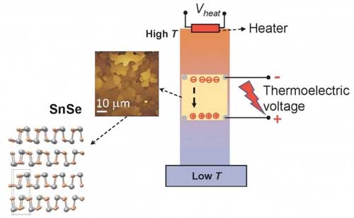 |
| Electric charges in a nanostructured tin selenide (SnSe) thin film flow from the hot end to the cold end of the material and generate a voltage. (Image: Xuan Gao)
|
|
Nanomaterials with nanometer-scale dimensions -- such as thickness and grain size -- have favorable thermoelectric properties. This inspired the researchers to grow nanometer-thick nanoflakes and thin films of SnSe to further study its thermoelectric properties.
|
|
The group’s work centers on the thermoelectric effect. They study how the temperature difference in a material can cause charge carriers -- electrons or holes -- to redistribute and generate a voltage across the material, converting thermal energy into electricity.
|
|
“Applying a voltage on a thermoelectric material can also lead to a temperature gradient, which means you can use thermoelectric materials for cooling,” said Gao. “Generally, materials with a high figure of merit have high electrical conductivity, a high Seebeck coefficient -- generated voltage per Kelvin of temperature difference within a material -- and low thermal conductivity,” he said.
|
|
A thermoelectric figure of merit, ZT, indicates how efficiently a material converts thermal energy to electrical energy. The group’s work focuses on the power factor, which is proportional to ZT and indicates a material’s ability to convert energy, so they measured the power factor of the materials they made.
|
|
To grow SnSe nanostructures, they used a chemical vapor deposition (CVD) process. They thermally evaporated a tin selenide powder source inside an evacuated quartz tube. Tin and selenium atoms react on a silicon or mica growth wafer placed at the low-temperature zone of the quartz tube. This causes SnSe nanoflakes to form on the surface of the wafer. Adding a dopant element like silver to SnSe thin films during material synthesis can further optimize its thermoelectric properties.
|
|
At the start, “the nanostructure SnSe thin films we fabricated had a power factor of only ~5 percent of that of single crystal SnSe at room temperature,” said Shuhao Liu, an author on the paper. But, after trying a variety of dopants to improve the material’s power factor, they determined that “silver was the most effective -- resulting in a 300 percent power factor improvement compared to undoped samples,” Liu said. “The silver-doped SnSe nanostructured thin film holds promise for a high figure of merit.”
|
|
In the future, the researcher hope that SnSe nanostructures and thin films may be useful for miniaturized, environmentally friendly, low-cost thermoelectric and cooling devices.
|

