| Posted: Apr 11, 2018 |
Researchers engineer new pathways for self-assembled nanostructures
(Nanowerk News) One way that scientists control the structure of materials at the nanoscale – where features are a few to several hundred nanometers (nm) – is by using “self-assembly,” in which molecules are designed such that they spontaneously come together to form a desired structure or pattern. Self-assembly is a powerful approach to controlling order at the nanoscale and is one way that scientists can design certain properties into a material for specific applications, such as solar energy conversion and storage.
|
|
Self-assembly is driven mainly by the system’s desire to minimize its energy and achieve equilibrium, but kinetic effects – the natural forces that move atoms and molecules around – can also play a strong role. Typically, these effects are viewed as complications to be overcome, but a collaboration of researchers from the U.S. Department of Energy’s (DOE) Brookhaven National Laboratory, Yale University, and the University of Warsaw (Poland) has recently shown that these effects can be exploited to engineer a nanostructure in a polymer thin film. Their results are published in the journal Nanoscale ("Pathway-engineering for highly-aligned block copolymer arrays").
|
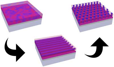 |
| At the beginning of the pathway engineering process, the block copolymer (purple and pink) are in complete disorder (top left). During photothermal shearing, the scientists use a laser beam to order the structure into horizontal tubes (middle). Finally, the scientists use conventional, high-temperature annealing to help the copolymers self-assemble into the desired pattern while maintaining the previously achieved order (top right). (Image: BNL)
|
|
The group worked with a type of polymer known as a block copolymer. Block copolymers are a well-studied and versatile class of self-assembling materials characterized by chemically distinct polymer blocks that are covalently bonded. This molecular architecture is what causes them to spontaneously form nanoscale patterns. In block copolymers, the covalent bonds frustrate the natural tendency of each individual polymer to remain separate (in general, different polymers, do not like to mix), so the material assembles into a nano-pattern instead.
|
|
At Brookhaven’s Center for Functional Nanomaterials (CFN)—a DOE Office of Science User Facility— the researchers started with a disordered block copolymer film mixed together with polymer chains. Conventionally, these films are then heated to allow the chains to move and assemble into an ordered pattern with nanoscale feature sizes. This traditional self-assembly approach generates precise nano-objects that are unfortunately not well organized into well-defined lattices over wide areas.
|
|
In this study the team used new processing methods developed at the CFN, taking the block copolymer film through very specific sequence that yielded self-assembled patterns that are significantly better ordered. These patterns were investigated at Brookhaven’s National Synchrotron Light Source II (NSLS-II), also a DOE Office of Science User Facility. This multi-step processing approach also allowed the group to control the block copolymer pattern orientation relative to the substrate, depending on the sequence of processing steps — a new concept that the scientists have termed “pathway engineering.”
|
|
“Applying the appropriate processing conditions to achieve a specific kind of order can be viewed as selecting a particular pathway through the self-assembly energy landscape,” said Kevin Yager, the group leader for Electronic Nanomaterials at CFN and one of the paper’s corresponding authors. “Pathway engineering allows us to bypass problematic energy barriers and access previously impossible structures.”
|
|
The first technique Yager and his group applied is called photothermal shearing, in which a focused laser beam is first swept through the film to generate a local hot zone that anneals the film and initiates the pattern self-assembly, accompanied by a “shear field” in the wake of the hot zone that forces the pattern to orient along a particular direction. A second step is conventional high-temperature annealing, which re-orients the self-assembled pattern while maintaining the previous directional alignment induced by the shear.
|
|
“The processing steps we apply may seem strange at first glance. We first order the material in a direction that we ultimately do not want. But the trick is that we can use this highly ordered intermediate state to template the pattern that we ultimately do want,” said first author Youngwoo Choo, a PhD student in Yale’s Department of Chemical and Environmental Engineering. “We identify a set of states that will move us towards the ultimate state that we want, and then select a sequence of processing protocols to step from one state to the next.”
|
|
Similarly, using only the shearing step does not yield the desired results. Choo’s advisor, co-author Chinedum Osuji, a materials scientist in the same department at Yale, explained, “While thin films of aligned horizontal cylinders can be obtained via shearing, it is not possible using shear alone to produce aligned vertical cylinders that are hexagonally packed.”
|
|
The group showed that the process of pathway engineering yields self-assembled patterns with nanoscale order even across substrates as large as a centimeter. They verified this using an x-ray technique called small-angle x-ray scattering, performed at NSLS-II’s Complex Materials Scattering (CMS) beamline. New techniques such as this that bridge between the nanoscale and the macroscale, provide useful tools for synthesis of advanced materials with tailored properties.
|

