If you’ve ever cracked open any type of electronic device, such as a PC or even a digital alarm clock, you would have discovered what is known as a printed circuit board (PCB). These typically green boards look like maps showing all of the electronic components of the device, including, what are known as conducting tracks. These tracks carry electric current, like rail road tracks, throughout the entire board so the device can operate. The boards also include insulating layers that shield the tracks from current leakage. Without these layers, even small electronic devices would require more energy to operate.
When evaluating the basic building blocks of that same PC or clock, but in molecular electronics, we would see a similar set-up with single molecules as conducting tracks and single electrons being transferred from the molecules. Whereas the insulating layer is helpful on the PCB, the similar underlying insulating substrate, at this scale, has further effects which need to be considered.
“While charging a molecule on an insulator, the atoms in the molecule will relax towards accommodating this additional charge and just as importantly, so will the nuclei in the insulator. Since the molecule is on top of an insulator, electronic characterization of such system is very difficult.” said Shadi Fatayer, a pre-doc at IBM Research and the first author of the paper.
He adds, “This change in the atoms’ position impacts their energy levels, which has drastic effects in terms of transferring a single-electron between molecules. The transfer rate of electrons could be tuned to vary several orders of magnitude.”
The team of scientists from IBM, University of Liverpool, Chalmers University and University of Regensburg tried a different approach to tackle this problem.
They first grew multilayers of NaCl, also known as sodium chloride or salt, serving as an insulating material, on top of a metal substrate. Such a system allows for the molecules that are absorbed on top to have their charge states stable and decoupled from the metal surface.
Then, the team pondered: “How do we measure reorganization energies?” Experimentally, it is done with molecules in solution, with molecules on top of a metal, but until now, there wasn’t a technique that allowed individual molecules on top of an insulator to be investigated.
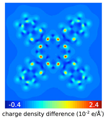
Their unique approach consists in employing the AFM and single electrons. Single electrons are used to probe charge state transitions of two defined charge-states in both directions. In the experiment the scientists test their method on a single naphthalocyanine molecule.
As previously published, the authors knew that they could reliably use the AFM to measure different charge states on top of an ultra-thin insulator with single electron sensitivity. They also recently demonstrated imaging of stably charged molecules as well as transferring single electrons between molecules on top of a thicker insulator. However, the ability to measure reorganization energies requires measuring the energy levels corresponding to particular charge-state transitions.
“Prior to this work, we knew how to measure the electric current though the molecule. However, this only worked in one direction for a given orbital. When we could measure the energy to attach an electron to a certain orbital, we could never measure the energy to remove one electron from that orbital and vice versa. The ability to measure in both directions – this was missing,” said IBM physicist Leo Gross. “With our AFM method, we measure the energy levels in both charge-state change directions on a thin film substrate. But it’s incredibly demanding work that deals with very weak signals, meaning many careful measurements are needed to perform proper statistical analysis.”
He adds, “Using this new methodology, we use the tip and the force exerted on the tip to count single electrons. We adjust the tip height and voltage and then count how long it takes for the one electron to go to (or from) the tip and from this you can obtain the energy levels.”
“Our biggest challenge was due to the tip being further away than normal to appropriately measure tunneling events,” adds Fatayer. “The very weak forces we measured associate to currents in the zepto Ampere scale – that’s 10 to the minus 21 (10-21). Most physicists don’t ever need to use this prefix, but we do it by measuring one electron every several seconds. We literally use the AFM as a single-electron current meter.”
While this is very fundamental research, the applications span from electronic devices, for example to characterization of defects in chips, to photovoltaics and organic semiconductors.