| Posted: Apr 19, 2018 |
New record on squeezing light to one atom: Atomic Lego guides light below one nanometer
(Nanowerk News) All electronic devices in our daily lives – computers, smartphones etc. – consist of billions of transistors, the key building block invented in Bell Labs in the late 1940s. The transistor started out being as big as 1cm, but thanks to advancement of technology, it has reached an amazing size of 14 nanometers, that is, 1000 times smaller than the diameter of a hair. At the same time, there has also been a race to further shrink devices that control and guide light. Light can function as an ultra-fast communication channel, for example between different sections of a computer chip, but it can also be used for ultra-sensitive sensors or novel on-chip nanoscale lasers.
|
|
New techniques have been on the rise searching for ways to confine light into extremely tiny spaces, millions of times smaller than current ones. Researchers had earlier on found that metals can compress light below the wavelength-scale (diffraction limit), but more confinement would always come at the cost of more energy losses. This paradigm has now been shifted, by using graphene instead!
|
|
In a recent study published in Science ("Probing the Ultimate Plasmon Confinement Limits with a van der Waals heterostructure"), ICFO researchers have been able to reach the ultimate level of confinement of light. That is, they have been able to confine light down to a space one atom thick in dimension, the smallest confinement ever possible. The work was led by ICREA Prof at ICFO Frank Koppens and carried out by David Alcaraz, Sebastien Nanot, Itai Epstein, Dmitri Efetov, Mark Lundeberg, Romain Parret, and Johann Osmond from ICFO, and performed in collaboration with University of Minho (Portugal) and MIT (USA).
|
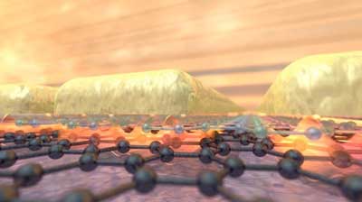 |
| This is an artistic impression of the squeezed light (plasmon) in between the metal and graphene, separated by just one a one-atom thick dielectric. (Image: ICFO)
|
|
The team of researchers used stacks (heterostructures) of 2D materials, and built up a completely new nano-optical device, as if it were atom-scale Lego. They took a graphene monolayer (semi-metal), and stacked onto it a hexagonal boron nitride (hBN) monolayer (insulator), and on top of this deposited an array of metallic rods. They used graphene because this material is capable of guiding light in the form of "plasmons", which are oscillations of the electrons, interacting strongly with light.
|
|
They sent infrared light through their devices and observed how the plasmons propagated in between the metal and the graphene. To reach the smallest space conceivable, they decided to reduce as much as possible the gap between the metal and the graphene to see if the confinement of light remained efficient, e.g. without additional energy losses. |
|
Strikingly enough, they saw that even when a monolayer of hBN was used as a spacer, the plasmons were still excited by the light, and could propagate freely while being confined to a channel of just on atom thick. They managed to switch this plasmon propagation on and off, simply by applying an electrical voltage, demonstrating the control of light guided in channels smaller than one nanometer of height.
|
|
The results of this discovery enable a completely new world of opto-electronic devices that are just one nanometer thick, such as ultra-small optical switches, detectors and sensors. Due to the paradigm shift in optical field confinement, extreme light-matter interactions can now be explored that were not accessible before. What is really exciting is that the atom-scale lego-toolbox of 2d materials has now also proven to be applicable for many types of completely new materials devices where both light and electrons can be controlled even down to the scale of a nanometer.
|

