| Posted: Apr 20, 2018 |
3D Nanoprinting facilitates communication with light
(Nanowerk News) At Karlsruhe Institute of Technology (KIT), researchers have developed a flexible and efficient concept to combine optical components in compact systems. They use a high-resolution 3D printing process to produce tiny beam-shaping elements directly on optical microchips or fibers and, hence, enable low-loss coupling. This approach replaces complicated positioning processes that represent a high obstacle to many applications today. The scientists present their concept in the Nature Photonics journal ("In situ 3D nanoprinting of free-form coupling elements for hybrid photonic integration").
|
|
In view of constantly growing data traffic, communication with light is gaining importance. For many years now, computing centers and worldwide telecommunication networks have been using optical connections for the quick and energy-efficient transmission of large amounts of data. The present challenge in photonics is to miniaturize components and to assemble them in compact and high-performance integrated systems suited for a variety of applications, from information and communication technologies to measurement and sensor technologies, to medical engineering.
|
 |
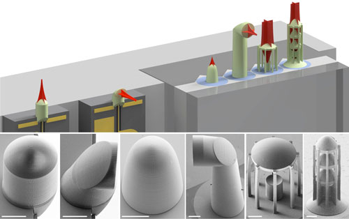
| Microlenses and micromirrors can be produced on optical fibers and microchips by 3D nanoprinting. This considerably facilitates assembly of photonic systems. (Image: Philipp-Immanuel Dietrich/Florian Rupp/Paul Abaffy, Karlsruhe Institute of Technology) (click on image to enlarge)
|
|
In this respect, hybrid systems are of very high interest. They combine a number of optical components with different functions. Hybrid systems offer superior performance and design freedom compared to monolithic integration concepts, for which all components are realized on a chip. Hybrid integration, for instance, allows individual optimization and testing of all components before they are assembled to a more complex system. Setup of optical hybrid systems, however, requires complex and expensive methods for the highly precise alignment of components and low-loss coupling of optical interfaces.
|
|
Researchers of KIT have how developed a new solution for the coupling of optical microchips to each other or to optical fibers. They use tiny beam-shaping elements that are printed directly onto the facets of optical components by a high-precision 3D printing process. These elements can be produced with nearly any three-dimensional shape and enable low-loss coupling of various optical components with a high positioning tolerance.
|
|
The researchers validated their concept in several experiments. They produced micrometer-sized beam-shaping elements of various designs and tested them on a variety of chip and fiber facets. As reported by the scientists in the journal Nature Photonics, they reached coupling efficiencies of up to 88% between an indium phosphide laser and an optical fiber. The experiments were carried out at the Institute of Microstructure Technology (IMT), the Institute of Photonics and Quantum Electronics (IPQ), and the Institute for Automation and Applied Informatics (IAI) of KIT, in cooperation with the Fraunhofer Institute for Telecommunications (Heinrich Hertz Institute, HHI) in Berlin and IBM Research in Zurich. The technology is presently being transferred to industrial application by Vanguard Photonics, a spinoff of KIT, under the PRIMA project funded by the Federal Ministry of Education and Research.
|
|
For the production of the three-dimensional elements, the researchers used multi-photon lithography: Layer by layer, a laser with an ultrashort pulse length writes the given structures into a photoresist that hardens simultaneously. In this way, 3D structures as small as a few hundred nanometers can be printed. Apart from microlenses, the process is also suited for producing other free-form elements, such as micromirrors, for the simultaneous adaptation of beam shape and propagation direction. In addition, complete multi-lens systems for beam expansion can be fabricated. With them, positioning tolerance during assembly of the components is enhanced.
|
|
“Our concept paves the way to automated and, hence, cost-efficient manufacture of high-performance and versatile optical hybrid systems,” says Professor Christian Koos, Head of IPQ and member of the Board of Directors of IMT as well as co-founder of Vanguard Photonics. “Hence, it essentially contributes to using the vast potential of integrated optics in industrial applications.”
|

