| Posted: May 14, 2018 |
Nano-ribbons from speeding nano-droplets(Nanowerk News) National University of Singapore (NUS) scientists have discovered a unique growth mechanism to produce atomically thin semiconductor ribbons that can serve as a building block for high-performance nanoelectronic devices (Nature Materials, "Vapor-Liquid-Solid Growth of Monolayer MoS2 Nanoribbons"). |
| Synthesis of ultrathin semiconductors, such as monolayer molybdenum disulphide and related compounds, has attracted tremendous interest in the past several years for their potential use in improving the performance of nanoelectronic devices. The ability to synthesise this emergent class of materials with a desired geometry would play an important role in facilitating their manufacturing process and implementation in high-density integrated circuits. |
| A team led by Prof Goki EDA from the Departments of Physics and Chemistry and the Centre for Advanced 2D Materials (CA2DM) at NUS has discovered a way to grow nano- and micro-ribbon structures of molybdenum disulphide that are only three atoms thick and on average hundreds of nanometers wide. The method involves the reaction of sulphur vapour with a mixture of molybdenum trioxide and sodium chloride salt at ~700°C on a clean crystal surface. |
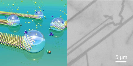 |
| (Left) Visual showing the growth of molybdenum disulphide nanoribbons mediated by liquid nano-droplets. (Right) Electron microscopy image showing oriented molybdenum disulphide micro- and nano-ribbons. (Image: NUS) |
| The researchers found that the salt reacts with molybdenum trioxide to yield a tertiary compound containing sodium, molybdenum and oxygen in various atomic ratios. This compound then melts and forms small droplets at the growth temperature (~700°C). The microscopic droplets of this compound then react with sulphur to form ultrathin ribbon-shaped molybdenum disulphide. This structure is strikingly different from the typical product of a salt-free growth, which is triangular and hexagonal in shape. |
| “The growth of ordered ribbons was a big surprise because the standard growth model does not predict such structures, but we realised that it was the result of a distinct growth mechanism,” said Dr LI, who was a research fellow in Prof Eda’s group but is now with the National Institute of Materials Science in Japan. The commonly accepted growth mechanism relies on the inherent dynamics of the precursors to diffuse and self-organise themselves on the substrate surface. Dr Li added, “This mechanism could not explain our observations.” |
| The researchers explain that the observed phenomenon is a form of the well-known vapour-liquid-solid (VLS) growth in which the vapour phase precursors condense into a liquid intermediate before forming the solid product. The morphology of the narrow ribbons obtained in this study was, however, unlike what is normally expected from a VLS growth, which typically yields cylindrical or tubular structures. Their observation indicates that the liquid droplet moves on the substrate surface in an ordered manner, leaving behind a track of ultrathin crystals. The process is similar to “painting with an ink droplet”. |
| The semiconducting ribbons synthesised by this method exhibited high crystal quality. The researchers demonstrated that high-performance microscopic transistors (with a field effect mobility of ~30 cm2/Vs and on-off ratio of ~106) can be fabricated from the individual ribbons. Because the as-synthesised material is already in the shape suitable for the device, this new growth method allows simple device fabrication without the need for an extra patterning step, which is normally required when other synthesis methods are used. |
| Prof Eda said, “Our work opens many interesting questions about surface and interface growth of nanomaterials. We believe that many other materials can be grown using a similar approach. The short-term goal is to understand the growth mechanism better and to control the morphology of the ribbons.” |
| Prof Eda envisions that the ability to directly grow complex semiconducting structures will greatly facilitate the realisation of high-performance nanoelectronic devices. |
| Source: National University of Singapore |

