| Posted: May 22, 2018 |
Leveraging imperfections to create better-behaved quantum dots
(Nanowerk News) Potentially paving the way toward advanced computers, lasers or optical devices, University of Wisconsin-Madison researchers have revealed new effects in tiny electronic devices called quantum dots.
|
|
In their work, published recently in the journal Nano Letters ("Mesoscopic Elastic Distortions in GaAs Quantum Dot Heterostructures"), the researchers developed and applied analysis methods that will help answer other challenging questions for developing electronic materials.
|
|
“We can now look at a set of structures that people couldn’t look at before,” says Paul Evans, professor of materials science and engineering at UW-Madison. “In these structures, there are new sets of crucial materials problems that we previously weren’t able to think about solving.”
|
|
The structures Evans and colleagues looked at are thousands of times narrower than single sheets of paper, and smaller than the dimensions of individual human cells. In those structures, quantum dots form inside very thin stacks of crystalline materials topped by an asymmetrical arrangement of flat, spindly, fingerlike metallic electrodes. Between the tips of those metallic fingers are small spaces that contain quantum dots.
|
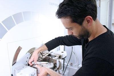 |
| Postdoctoral scholar Anastasios Pateras adjust an X-Ray instrument used to detect previously unknown defects in quantum dots. (Image: Sam Million-Weaver)
|
|
Creating such precise structures and peering inside those tiny spaces is technically challenging, however, and quantum dots don’t always behave as expected.
|
|
Previous work by Evans’ collaborators at the Delft University of Technology in the Netherlands, who created and extensively studied the crystal stack structures, led to suspicions that the quantum dots were different in important ways from what had been designed.
|
|
Until now, measuring those differences wasn’t possible.
|
|
“Previous imaging approaches and the modeling weren’t allowing people to structurally characterize quantum dot devices at this tiny scale,” says Anastasios Pateras, a postdoctoral scholar in Evans’ group and the paper’s first author.
|
|
Pateras and colleagues pioneered a strategy for using beams of very tightly focused X-rays to characterize the quantum dot devices—and that hinged on a new method for interpreting how the X-rays scattered. Using their approach, they observed shifts in the spacing and orientation of atomic layers within the quantum dots.
|
|
“Quantum dots need to be close to perfect,” says Evans. “This small deviation from perfection is important.”
|
|
The team’s discovery indicates that the process of creating the quantum dots—laying down metallic electrodes atop a lab-grown crystal—distorts the material underneath slightly. This puckering creates strain in the material, leading to small distortions in the quantum dots. Understanding and exploiting this effect could help researchers create better-behaved quantum dots.
|
|
“Once you know these quantities, then you can design devices that take into account that structure,” says Evans.
|
|
Designs with those small imperfections in mind will be especially important for future devices where many thousands of quantum dots must all work together.
|
|
“This is going to be very relevant because, right now, there are multiple sources of decoherence quantum dots,” says Pateras.
|
|
The researchers now are developing an algorithm to automatically visualize atomic positions in crystals from X-ray scattering patterns, given that performing the necessary calculations by hand would likely be too time-consuming. Additionally, they are exploring how the techniques could add insight to other hard-to study structures.
|

