| Posted: May 23, 2018 |
Understanding the generation of light-induced electrical current in atomically thin nanomaterials
(Nanowerk News) Scientists at the Center for Functional Nanomaterials (CFN)—a U.S. Department of Energy (DOE) Office of Science User Facility at Brookhaven National Laboratory—have used an optoelectronic imaging technique to study the electronic behavior of atomically thin nanomaterials exposed to light. Combined with nanoscale optical imaging, this scanning photocurrent microscopy technique provides a powerful tool for understanding the processes affecting the generation of electrical current (photocurrent) in these materials. Such an understanding is key to improving the performance of solar cells, optical sensors, light-emitting diodes (LEDs), and other optoelectronics—electronic devices that rely on light-matter interactions to convert light into electrical signals or vice versa.
|
|
“Anyone who wants to know how light-induced electrical current is distributed across a semiconductor will benefit from this capability,” said CFN materials scientist Mircea Cotlet, co-corresponding author on the Advanced Functional Materials paper describing the work ("Distinct Optoelectronic Signatures for Charge Transfer and Energy Transfer in Quantum Dot–MoS2 Hybrid Photodetectors Revealed by Photocurrent Imaging Microscopy").
|
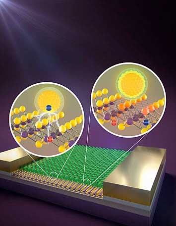 |
| A field-effect transistor (the device) containing molybdenum disulfide (stick and balls) doped with core-only quantum dots undergoing charge transfer (left zoom; charge transfer is shown as sparks) and core/shell quantum dots undergoing energy transfer (right zoom; energy transfer is shown as a wave moving from the quantum dots to molybdenum disulfide). (Image: Brookhaven National Laboratory)
|
Generating an electrical current
|
|
When hit with light, semiconductors (materials that have an electrical resistance in between that of metals and insulators) generate an electric current. Semiconductors that consist of one layer or a few layers of atoms—for example, graphene, which has a single layer of carbon atoms—are of particular interest for next-generation optoelectronics because of their sensitivity to light, which can controllably alter their electrical conductivity and mechanical flexibility. However, the amount of light that atomically thin semiconductors can absorb is limited, thus limiting the materials’ response to light.
|
|
To enhance the light-harvesting properties of these two-dimensional (2D) materials, scientists add tiny (10–50 atoms in diameter) semiconducting particles called quantum dots in the layer(s). The resulting “hybrid” nanomaterials not only absorb more light but also have interactions occurring at the interface where the two components meet. Depending on their size and composition, the light-excited quantum dots will transfer either charge or energy to the 2D material. Knowing how these two processes influence the photocurrent response of the hybrid material under different optical and electrical conditions—such as the intensity of the incoming light and applied voltage—is important to designing optoelectronic devices with properties tailored for particular applications.
|
|
“Photodetectors sense an extremely low level of light and convert that light into an electrical signal,” explained Cotlet. “On the other hand, photovoltaic devices such as solar cells are made to absorb as much light as possible to produce an electrical current. In order to design a device that operates for photodetection or photovoltaic applications, we need to know which of the two processes—charge or energy transfer—is beneficial.”
|
Lighting up charge and energy transfer processes
|
|
In this study, the CFN scientists combined atomically thin molybdenum disulfide with quantum dots. Molybdenum disulfide is one of the transition-metal dichalcogenides, semiconducting compounds with a transition-metal (in this case, molybdenum) layer sandwiched between two thin layers of a chalcogen element (in this case, sulfur). To control the interfacial interactions, they designed two kinds of quantum dots: one with a composition that favors charge transfer and the other with a composition that favors energy transfer.
|
|
“Both kinds have cadmium selenide at their core, but one of the cores is surrounded by a shell of zinc sulfide,” explained CFN research associate and first author Mingxing Li. “The shell is a physical spacer that prevents charge transfer from happening. The core-shell quantum dots promote energy transfer, whereas the core-only quantum dots promote charge transfer.”
|
|
The scientists used the clean room in the CFN Nanofabrication Facility to make devices with the hybrid nanomaterials. To characterize the performance of these devices, they conducted scanning photocurrent microscopy studies with an optical microscope built in-house using existing equipment and the open-source GXSM instrument control software developed by CFN physicist and co-author Percy Zahl. In scanning photocurrent microscopy, a laser beam is scanned across the device while the photocurrent is measured at different points. All of these points are combined to produce an electrical current “map.” Because charge and energy transfer have distinct electrical signatures, scientists can use this technique to determine which process is behind the observed photocurrent response.
|
|
The maps in this study revealed that the photocurrent response was highest at low light exposure for the core-only hybrid device (charge transfer) and at high light exposure for the core-shell hybrid device (energy transfer). These results suggest that charge transfer is extremely beneficial to the device functioning as a photodetector, and energy transfer is preferred for photovoltaic applications.
|
|
“Distinguishing energy and charge transfers solely by optical techniques, such as photoluminescence lifetime imaging microscopy, is challenging because both processes reduce luminescence lifetime to similar degrees,” said CFN materials scientist and co-corresponding author Chang-Yong Nam. “Our investigation demonstrates that optoelectronic measurements combining localized optical excitation and photocurrent generation can not only clearly identify each process but also suggest potential optoelectronic device applications suitable to each case.”
|
|
“At the CFN, we conduct experiments to study how nanomaterials function under real operating conditions,” said Cotlet. “In this case, we combined the optical expertise of the Soft and Bio Nanomaterials Group, device fabrication and electrical characterization expertise of the Electronic Nanomaterials Group, and software expertise of the Interface Science and Catalysis Group to develop a capability at the CFN that will enable scientists to study optoelectronic processes in a variety of 2D materials. The new scanning photocurrent microscopy facility is now open to CFN users, and we hope this capability will draw more users to the CFN fabrication and characterization facilities to study and improve the performance of optoelectronic devices.”
|

