| Posted: Jun 08, 2018 |
Light-bending nano-patterns for LEDs
(Nanowerk News) Nanoscale patterns designed to bend, deflect and split light can now be fabricated directly on light-emitting diode (LED) surfaces using an innovative etching method developed by A*STAR researchers (Applied Physics Letters, "High-efficiency and low-loss gallium nitride dielectric metasurfaces for nanophotonics at visible wavelengths"). The new fabrication scheme creates new possibilities for the facile control of light output.
|
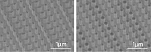 |
| Nanopillar arrays fabricated directly on a GaN surface. (Image: A*STAR Data Storage Institute)
|
|
Recent advancements in LED lighting have transformed daily life and cutting-edge technology — from efficient room lighting, to TV and mobile device backlights, and the tiny optical circuits that drive global fiber-optic networks.
|
|
The light-emitting component of LEDs is a surprisingly simple structure, typically a thin layer of a dielectric material such as gallium nitride (GaN) on a crystalline sapphire substrate. This structure means the light emitted by LEDs is inefficiently dispersed in all directions, including back into the substrate on which the light-emitting layer is fixed. So, while researchers have made tremendous advances in light-emitting efficiency, there remains room for improvement.
|
|
Egor Khaidarov and colleagues from A*STAR’s Data Storage Institute and Nanyang Technological University have now found a way to pattern GaN with nanoscale features that can control the behavior of light.
|
|
“We have demonstrated that metasurfaces — surfaces patterned with features typically smaller than the wavelength of emitted light — can be fabricated directly on a standard GaN-on-sapphire platform,” says Khaidarov. “Most importantly, we have shown that with good design, it is possible to create the metasurfaces without the need for an additional layer, while still maintaining a high level of emission efficiency.”
|
|
Metasurface modifications of LEDs have been attempted in the past. These included patterning an additional layer with a very different refractive index than the underlying GaN-on-sapphire substrate to keep the light in the metasurface layer and enhance the light-matter interactions. The problem with patterning GaN directly — a major benefit for fabrication — is a weakness of interactions because of the lack of refractive index contrast.
|
|
“To overcome this, we worked with very deep structures with a large aspect ratio, effectively arrays of nanopillars, to reduce the influence of the substrate on the metasurface’s optical modes,” explains Khaidarov (see image).
|
|
The resulting design, however, posed a major challenge for fabrication, requiring the team to develop a precise nanofabrication procedure involving electron beam lithography and fast, high-temperature reactive ion etching.
|
|
“With our design concept we have, in principle, full control of the output properties of light, which allows us to fabricate more complex optical components such as lenses, vortex beam generators, polarimeters and holograms,” says Khaidarov.
|

