| Posted: Jun 15, 2018 |
Scientists make an important step towards the control of excitonic effects in 2D van der Waals heterostructures(Nanowerk News) An international team of scientists, including NUST MISIS's Professor Gotthard Seifert, have made an important step towards the control of excitonic (lat. excito -- «excite») effects in two-dimensional van der Waals heterostructures. In the future, this research will help to create electronics with more controlled properties. The research has been published in Nature Physics. |
| The creation of two-dimensional semiconductor materials is one of the most important areas of modern materials science. These materials can be the basis for elements needed to create the next generation of electronics. |
| One two-dimensional material with suitable electronic characteristics is two-dimensional molybdenum disulfide (MoS2), which has a single-layer structure (one atom layer) of molybdenum located between two sulfur layers: this material has a high charge mobility and high on/off in the transistor element. |
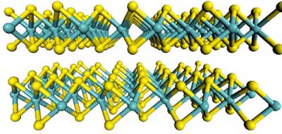 |
| These are molybdenum atoms. (Image: NUST MISIS) |
| In 2017, Professor Gotthard Seifert described the mechanism of defect germination in the structure of two-dimensional molybdenum disulfide as a process that will make it possible for scientists to capitalize on two-dimensional MoS2's full potential use in microelectronics. This work was published in ACS Nano ("Momentum-space indirect interlayer excitons in transition-metal dichalcogenide van der Waals heterostructures"). |
| The study of other two-dimensional materials' properties for their application in electronics has become the next step in this field. Monolayers of molybdenum disulfide (and, for example, wolframite diselenides--WSe2) have shown exceptional optical properties due to excitons: tightly bound pairs of electron-hole (quasiparticles acting as a carrier of a positive charge). |
| At the same time, the creation of the MoS2/WSe2 heterostructure by laying separate monolayers on each other leads to the appearance of a new type of exciton in it, where the electron and the hole are spatially divided into different layers. |
| Scientists have shown that interlayer excitons give a very specific optical signal display when layered. This allow scientists to study quantum phenomena, making it ideal for experiments in volitronics (a field of quantum electronics, «valley», or the local minimum of an element's conduction zone) to control electrons in the «valleys» of semiconductors. In the future, these breakthroughs could lead to the most effective way to code information (by placing an electron in one of these valleys). |
| "Thanks to the use of spectroscopic methods and quantum-chemical calculations from the first principles, we have revealed a partially charged electron-hole in MoS2/WSe2 heterostructures, as well as [the electron-hole's] location. We have managed to control the radiation energy of this new exciton by changing the relative orientation of the layers", commented Professor Gotthard Seifert, one of NUST MISIS`s leading scientists. |
| According to Seifert, this result is an important step towards understanding and controlling exciton effects in Van der Waals heterostructures (where these distance-dependent atomic interactions occur). The research team is continuing to study the effect of layer rotations on the material's electronic properties. In the future, this will allow for the creation of unique new materials for solar panels or electronics. |
| Source: National University of Science and Technology MISIS |

