| Posted: Jun 22, 2018 |
Insulator-metal transition at the nanoscale: x-ray holography reveals existence of nano-patchwork
(Nanowerk News) Controlling the flow of electrons within circuits is how electronic devices work. This is achieved through the appropriate choice of materials. Metals allow electrons to flow freely and insulators prevent conduction. In general, the electrical properties of a material are determined when the material is fabricated and cannot be changed afterwards without changing the material. However, there are materials that can exhibit metal or insulator behaviour depending on their temperature. Being able to switch their properties, these materials could lead to a new generation of electronic devices.
|
|
Vanadium Dioxide (VO2) is one such material. It can switch from an insulating phase to a metallic phase just above room temperature, a feature exploited already for sensors. However, the reason why the properties of this material change so dramatically has been a matter of scientific debate for over 50 years.
|
|
One of the challenges in understanding why and how this switch occurs is due to a process called phase separation. The insulator-metal phase transition is similar to the ice to liquid transition in water. When ice melts, both liquid and solid water can coexist in separate regions. Similarly, in VO2, insulating and metallic regions of the material can be coexisting at the same time during the transition.
|
|
But unlike water, where the different regions are often large enough to see with the naked eye, in VO2 this separation occurs on the lengthscale of nanometers and it is thus challenging to observe. As a result, it has been hard to know if the true properties of each phase, or the mixture of both phases, are being measured.
|
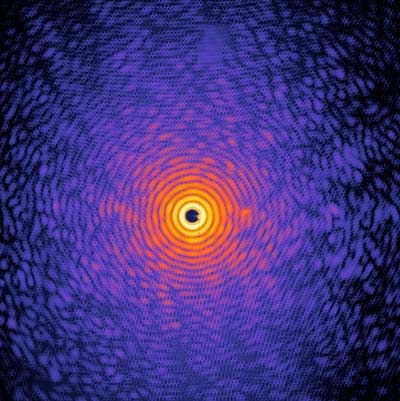 |
| Fig. 1: X-ray hologram of VO2 during the phase Transition. (Image: MBI)
|
|
X-rays are a key tool for understanding the properties of materials, but it has been hard to use them to tackle this problem as this requires the combination of nanometer spatial resolution with a spectroscopic sensitivity allowing to discriminate the different phases in an image. However, in a recent study published in Nano Letters ("Imaging Nanometer Phase Coexistence at Defects During the Insulator–Metal Phase Transformation in VO2 Thin Films by Resonant Soft X-ray Holography"), a team of researchers from the Max Born Institute and the Technische Universität in Berlin, Institute for Photonic Sciences and ALBA in Barcelona, as well as Vanderbilt University in Tennessee, has finally been able to probe the phase transitions that occur in thin films of VO2 using resonant soft X-ray holography.
|
|
This imaging technique is capable of tracing and imaging the electronic and structural changes in this material with a spatial resolution of about 40 nanometers - that is 500.000 times smaller than your typical ice cube in a drink.
|
|
By looking at microscopic vanadium dioxide crystal platelets, the scientists were able to observe that defects in the material played an important role in initiating the phase transition from the insulator to the metal. However, more importantly, the authors also observed a third intermediate state formed during the phase transformation.
|
|
Whilst some regions transformed directly from the insulating to metallic phase, others transformed into a second different insulating state before becoming metallic at higher temperatures, with the exact pathway taken depending on the defects present in the material. The coexistences of three phases has radically changed the view based on previous studies that assumed the presence of only two states during the transition.
|
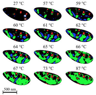 |
| Fig. 2: Nano-patchwork of different domains forming at different temperatures (in degree Kelvin) during the phase transition, obtained by series of x-ray holograms such as the one shown in Fig.1. The different domains and defects in the VO2 crystallites are shown in false color to represent their different properties. red = defect region, black = insulating M1 phase, blue = newly observed insulating M2 phase, green = metallic R phase. The 500 nanometer scale bar amounts to about 1/100 of the diameter of a human hair. (Image: MBI/ICFO)
|
|
In the future, the scientists want to trigger the phase transition with ultrashort laser pulses and observe the dynamics of the transition. “As the material naturally wants to form this patchwork of different domains during the transition from insulator to metal, we need to observe how this process unfolds in time to understand and better control it in the future”, says Prof. Stefan Eisebitt from the Max Born Institute in Berlin.
|
|
Key to this endeavour are the unique possibilities that X-ray holography brings to the study materials on the nanoscale. Exploiting the coherence and ultrashort pulses of x-ray lasers such as the recently inaugurated European X-Ray Free Electron Laser (XFEL), x-ray holography is one of the very few methods that can really image the dynamics of ultrafast processes which occur within femto- and picoseconds in a solid material.
|
|
“We are really excited about the prospect of recording a movie of how the phase transition proceeds, reflecting the interplay of atomic nuclei and electrons in the different domains of a sample”, says Prof. Simon Wall from the Institute of Photonic Sciences in Barcelona. “Beyond vanadium dioxide, this approach will help us to fundamentally understand the properties of many intriguing materials, including for example high temperature superconductors.”
|

