| Posted: Jun 25, 2018 |
No barrier to applications for a remarkable 2D material
(Nanowerk News) Mass production of large, uniform sheets of single-layer molybdenum disulfide, MoS2, is difficult, which limits its commercial application. A*STAR researchers have modified an existing manufacturing technique to enable the use of MoS2 in a range of technologies from photodevices to flexible, transparent sensors (ACS Nano, "Modification of vapor phase concentrations in MoS2 growth using a NiO foam barrier").
|
|
The two-dimensional material has attracted considerable attention because of its extraordinary physical, electronic and optoelectronic properties, including flexibility, transparency and semiconducting characteristics. But fabricating large-scale, defect-free single layers of MoS2 is highly challenging.
|
|
Dongzhi Chi and his team from the A*STAR Institute of Materials Research and Engineering, in collaboration with colleagues from the National University of Singapore and the Indian Institute of Science Education and Research, has modified a current technique, known as chemical vapor deposition (CVD), so that it can now produce uniform, centimeter-sized sheets of MoS2 crystals with large grain sizes.
|
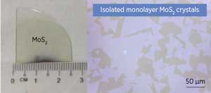 |
| Two-dimensional monolayer MoS2 was grown on sapphire (left). The optical microscope image on the right shows isolated monolayer MoS2 crystals at the periphery of the film. (© ACS)
|
|
“The physical properties of MoS2 vary greatly with its thickness,” explains Chi, “to maintain its remarkable electronic and physical properties we need a method that can uniformly deposit MoS2 films over a large area with high crystallinity.”
|
|
Although CVD is an effective technique for fabricating large-area, uniform sheets of MoS2 of varying thickness on different substrates, and significant progress has been made in improving the quality of MoS2 monolayers produced by the technique, little attention has been paid to controlling the chemical vapors using physical barriers during the growth of MoS2 crystals.
|
|
By introducing a nickel oxide (NiO) barrier, the researchers were able to control the concentration and distribution of chemical vapors during the growth of MoS2 crystals. Because NiO reacts with molybdenum trioxide (MoO3), one of the chemical reactants used in the growth process, it traps and lowers the MoO3 concentration, allowing the uniform deposition of monolayers of MoS2 over a large area.
|
|
“The advantage of this approach is the ease of implementation as well as a reduction in contamination, and it allows for control of the chemical exposure during the growth process,” says Chi.
|
|
The work has led to further advances in the fabrication of uniform and large-area MoS2 monolayers, and could also be applied to other two-dimensional materials.
|
|
“We are now looking to scale up our fabrication process for producing even larger sheets, which could pave the way for next-generation optoelectronic and sensor technologies,” says Chi.
|

