| Jul 09, 2018 |
Manipulating single atoms in graphene with an electron beam(Nanowerk News) The same electrons that form images of atomic structures can also be used to move atoms in materials. This technique of single-atom manipulation, pioneered by University of Vienna researchers, is now able to achieve nearly perfect control over the movement of individual silicon impurity atoms within the lattice of graphene, the two-dimensional sheet of carbon. |
| The latest results are reported in the scientific journal Nano Letters ("Electron-Beam Manipulation of Silicon Dopants in Graphene"). |
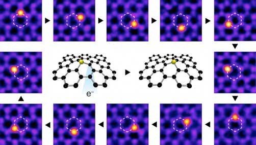 |
| An electron beam focused on a carbon atom next to a silicon impurity atom can controllably make it jump to where the beam was placed. Step by step this allows the silicon to be moved with atomic precision around a hexagonal path. (Image: CC-BY, Toma Susi / University of Vienna) |
| As an epoch-making achievement in nanotechnology, the scanning tunneling microscope has since the late 1980s been able to move atoms over surfaces, and has until very recently been the only technology capable of moving individual atoms in such a controlled manner. |
| Now, the scanning transmission electron microscope (STEM) is able to reliably focus an electron beam with sub-atomic precision, allowing scientists to directly see each atom in two-dimensional materials like graphene, and also to target single atoms with the beam. Each electron has a tiny chance of scattering back from a nucleus, giving it a kick in the opposite direction. |
| Building on work published over the past few years, a research team at the University of Vienna led by Toma Susi has now used the advanced electron microscope Nion UltraSTEM100 to move single silicon atoms in graphene with truly atomic precision. Even with manual operation, the achieved movement rate is already comparable to the state-of-the-art in any atomically precise technique. |
| "The control we are able to achieve by essentially directing the electron beam by hand is already remarkable, but we have further taken the first steps towards automation by detecting the jumps in real time", says Susi. |
| The new results also improve theoretical models of the process by including simulations by collaborators in Belgium and Norway. |
| In total, the researchers recorded nearly 300 controlled jumps. Additional to extended paths or moving around a single hexagon made of carbon atoms in graphene, a silicon impurity could be moved back and forth between two neighboring lattice sites separated by one tenth-billionth of a meter, like flipping an atomic-sized switch. In principle, this could be used to store one bit of information at record-high density. |
| Dr. Susi concludes, "Your computer or cellphone will not have atomic memories anytime soon, but graphene impurity atoms do seem to have potential as bits near the limits of what is physically possible." |
| Source: University of Vienna |
|
Subscribe to a free copy of one of our daily Nanowerk Newsletter Email Digests with a compilation of all of the day's news. |

