| Jul 11, 2018 |
On the path to new high-performance transistors(Nanowerk News) The electronics industry expects a novel high-performance transistor made of gallium nitride to offer considerable advantages over present-day high-frequency transistors. Yet many fundamental properties of the material remain unknown. |
| Now, for the first time, researchers at the Paul Scherrer Institute PSI have observed electrons while they were flowing in this promising transistor. For that they used the world's top-performing source of soft X-rays at PSI's Swiss Light Source SLS. This unique experiment was conducted by PSI researchers together with colleagues from Russia and Romania. |
| Their finding: When going into the high power regime of the gallium nitride transistor, in specific directions the electrons move more efficiently. This insight will help to develop faster and more powerful transistors – a prerequisite for converting our communication network to the coming 5G standard. |
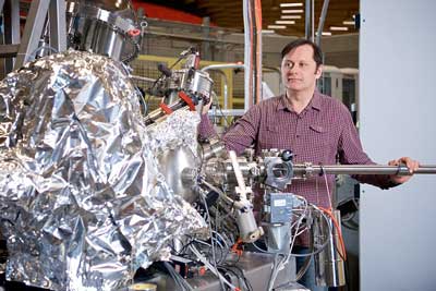 |
| Vladimir Strocov at the ADRESS-Beamline of the Swiss Light Source SLS, where the experiments took place. This ist the world's most intense source for soft X-ray radiation. (Image: Paul Scherrer Institute/Markus Fischer) |
| The researchers have now published their results in the journal Nature Communications ("k-space imaging of anisotropic 2D electron gas in GaN/GaAlN high-electron-mobility transistor heterostructures"). |
| For smartphones and more broadly for the mobile communication technology of the near future, a new generation of semiconductor components is urgently needed: Today's prevalent 3G/4G standard for mobile communication is running up against its performance limits. Its successor, 5G, is supposed to be commercially available by 2020. This standard will offer higher frequencies (up to 100 gigahertz), higher data rates (up to 20 Gb/s), higher network densities, and more efficient use of energy. |
| However, the more powerful high-frequency transmitters required for this cannot be realised using traditional transistors and conventional semiconductor technology. Therefore researchers around the world are working on an alternative: HEMT devices – high-electron-mobility transistors – based on gallium nitride. In a HEMT electrons can move freely in a layer one-millionth of a millimetre thick between two semiconductors. |
| In their experiment, PSI researcher Vladimir Strocov and his colleagues looked into the question of how one might, through clever construction of a HEMT, contribute to an optimal flow of electrons. Their finding: When going into the high power regime of the gallium nitride transistor, in specific directions the electrons move more efficiently. |
Freedom for electrons |
| Semiconductors are the basic building blocks of all miniaturised circuitry and computer chips. They conduct electricity only when they are skillfully prepared. In classical semiconductor components such as transistors, that is accomplished through selective incorporation of atoms of a complementary chemical element. The problem is that these foreign atoms slow down the electron motion. |
| In the HEMT, this problem is solved in an elegant way. Here, in something like a sandwich, a suitable combination of pure semiconductor materials is brought into contact so that, at the boundary, a conducting layer one-millionth of a millimetre thick is formed. That makes it possible to do without the foreign atoms. |
| This idea, first proposed in the early 1980s by the Japanese scientist Takashi Mimura, is already used today in the high-frequency circuits of all smartphones. In practice, however, it is also relevant that the atoms in a semiconductor are always arranged in a specific periodic crystal structure. |
| For example, the HEMT that Strocov and his team studied, made from aluminium nitride and gallium nitride, has a six-fold symmetry in its interface layer: There are six equivalent orientations along the atomic chains. |
| To investigate the flow of electrons within the interface layer, the researchers placed their HEMT under a very special microscope – one that does not examine the positions, but rather the propagation speeds of the electrons: the ADRESS beamline of the Swiss Light Source SLS, the world's most intense source for soft X-ray radiation. |
Experiment on a living transistor |
| The technical concept of this examination method is called angle-resolved photoelectron spectroscopy, or ARPES. Up to now it has been carried out with light sources in the ultraviolet range. Now Strocov and his team have used the high-energy X-ray light of SLS to do it. With it, the researchers were able to lift out electrons from deep inside the conducting layer of the HEMT and then guide them into a measuring instrument that determined their energy, speed, and direction: an experiment on a living transistor, so to speak. |
| That is the first time it has been possible to make the fundamental properties of electrons in a semiconductor heterostructure visible, says Vladimir Strocov. |
Performance boost for mobile communication networks |
| The high intensity of the X-rays at SLS – which far outperforms comparable facilities – was crucially important for this, acknowledge Leonid Lev and Ivan Maiboroda of the Kurchatov Institute in Russia, where the HEMT devices were fabricated: The unique instrumentation of SLS provided us with extremely important scientific results. It showed us ways in which HEMT structures with higher operating frequencies and performance could be developed. |
| The fact that the electrons prefer a particular direction of flow can be exploited technically, Strocov explains: If we orient the atoms in the gallium nitride HEMT so that they match the electrons' direction of flow, we get a significantly faster and more powerful transistor. |
| The consequence is a performance boost for 5G technology. The gallium-nitride HEMTs the scientists have now investigated are already predicted to have a great future in the development of new transmitters. With the present insights from their experiment, the reserachers estimate, the performance of radio transmitters could be increased yet again by around ten percent. |
| For mobile communication networks, this means fewer transmitter stations would be required to provide the same network coverage and power – and with that, reductions worth millions in maintenance and energy costs. |
| Source: Paul Scherrer Institut |
|
Subscribe to a free copy of one of our daily Nanowerk Newsletter Email Digests with a compilation of all of the day's news. |

