| Jul 16, 2018 |
A silicon-nanoparticle photonic waveguide(Nanowerk News) A new way to efficiently guide light at tiny scales has been demonstrated by an all-A*STAR team (Nano Letters, "Resonant light guiding along a chain of silicon nanoparticles"). Their method, which involves lining up silicon nanoparticles, is promising for applications such as light-based integrated circuits, biosensors and quantum communications. |
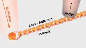 |
| Near-field scanning optical microscope (NSOM) measurements have shown that cylindrical silicon nanoparticles arranged in a line can transport light with low loss due to magnetic-field (H-field) resonances between them. (© ACS) |
| Transporting light on small scales is critical for many applications and is commonly performed using rectangular silicon waveguides — the optical circuit equivalent to wires in electronic circuits. To further shrink devices, metallic nanoparticles have been explored as an alternative, but while they are very good at confining light to small scales, they tend to leak a lot of the light. |
| Now, Reuben Bakker, Arseniy Kuznetsov and their colleagues at the A*STAR Data Storage Institute have come up with a more efficient method that involves a string of cylindrical silicon nanoparticles. The first nanoparticle is excited using light and then a near-field scanning optical microscope measures the light that reaches another nanoparticle further down the line (see image). When they did this, the team found that the fall in the light intensity was low. |
| “This is the first experimental demonstration that shows coupled resonators can very efficiently guide light at strongly sub-wavelength dimensions and over lengths of several hundred micrometers,” says Kuznetsov. “It’s the first step toward a completely new approach to silicon photonics.” |
| The nanoparticles are not in direct contact with each other. Instead, light is transferred to the next particle through magnetic-field resonances. “Each of these particles is a resonant scatterer — so if you take one particle it will scatter light in all directions,” explains Kuznetsov. “But when we line all these particles up, they work as a single waveguide without leaking light.” |
| One big advantage of using silicon nanoparticles is that they are compatible with the fabrication processes currently used by the semiconductor industry. “You can use the same CMOS processes to do silicon photonics,” says Kuznetsov. “You just change the mask and the layout and add other components without any additional complications.” |
| Despite having modeled the system and its behavior as a waveguide before performing the measurements, the team were still amazed at how well it worked in practice. “We were surprised it worked so well,” recalls Bakker. “We tweaked the geometries a little bit, but to have them perform so well after just a few iterations was quite unexpected.” |
| The team has already demonstrated the same concept at telecommunication wavelengths. They are now working on developing various on-chip photonic components based on the concept. |
| Source: A*STAR |
|
Subscribe to a free copy of one of our daily Nanowerk Newsletter Email Digests with a compilation of all of the day's news. |

