| Jul 16, 2018 |
Brighter microscopy using built-in nanobulbs(Nanowerk News) By using ultrafast laser pulses to join silicon and gold atoms into a new type of nanoparticle, researchers from A*STAR and ITMO University, Russia, have created a white-light source for applications including high-resolution characterization of biomolecules (Nano Letters, "Nanoscale generation of white light for ultrabroadband nanospectroscopy"). |
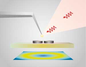 |
| Schematic of a functionalized nanotip for ultrabroadband nanospectrometry. (© ACS) |
| The wave nature of light imposes constraints on the resolution of conventional optical microscopes, no matter how intense the source. The process of diffraction spreads out light waves at the nanoscale and produces blurry images when objects are smaller than half the source beam’s wavelength. |
| Now, researchers have devised a way to beat the diffraction limit. Arseniy Kuznetsov and Yefeng Yu from the A*STAR Data Storage Institute have teamed up with colleagues at Russia’s ITMO University to improve near-field scanning optical microscopy (NSOM) devices. These microscopes embed optically active materials inside a sharp microscale tip. When positioned extremely close to a sample, the light-emitting tip generates evanescent waves capable of resolving items separated by just a few nanometers. |
| One drawback of NSOM is that implanted light sources, such as quantum dot crystals and photoactive molecules, tend to emit in narrow regions of the electromagnetic spectrum. This makes it difficult to use these materials for emerging ‘nanospectroscopy’ applications that detect a sample’s structural and optical features in ultra-fine detail; broad-spectrum white light that excites many components of a specimen simultaneously would be preferable. |
| Kuznetsov, Yu, and their colleagues realized that silicon nanoparticles, which exhibit wide-ranging luminescence after laser excitation, might solve this white light problem if they could be made more efficient at scales suitable for NSOM tips. To realize this goal, the team deposited a thin layer of silicon on top of a gold-coated substrate, and then exposed the material to bursts of ultra-fast lasers. Spherical silicon nanoparticles containing integrated gold regions were recovered from the ablation process. |
| “Normally, these two materials are unmixable — melting them together won’t produce a good alloy,” explains Kuznetsov. “But when the process happens with femtosecond laser pulses, we get a hybrid that solidifies in an unusual state.” |
| The researchers’ experiments revealed that the gold regions of the new material produced high-energy, ‘hot’ electrons that transferred to silicon crystals and helped them emit ultraviolet, visible, and infrared light. Attaching the hybrid particle to the end of a microscopic tip enabled them to scan nanoscale photonic devices and map out their optical response at high speeds. |
| “This mixture has unique photoluminescence properties that take advantage of both components,” says Kuznetsov. “We are working on ways to control their dimensions and nanocompositions.” |
| Source: A*STAR |
|
Subscribe to a free copy of one of our daily Nanowerk Newsletter Email Digests with a compilation of all of the day's news. |

