| Jul 18, 2018 |
Steering light with dynamic lens-on-MEMS(Nanowerk News) A new class of flat, ultrathin optical devices on a chip was developed by scientists from the Center for Nanoscale Materials at Argonne National Laboratory and Harvard University (APL Photonics, "Dynamic metasurface lens based on MEMS technology"). |
| The new design uses a microscopic electromechanical device (MEMS) as a platform. The design imparts dynamic and high-speed control to an optical lens for actively steering light. |
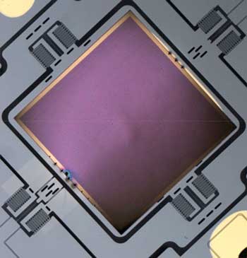 |
| Optical microscope image of a lightweight, flat lens on a micro-electromechanical scanner. The mirror dimensions are 1 millimeter by 1 millimeter with a thickness of 10 microns. Integration of the micro-electromechanical devices with advanced flat optical surfaces will help create a new paradigm to manipulate light by combining the strength of high-speed dynamic control and precise spatial manipulation of light properties. (Image: Center for Nanoscale Materials at Argonne National Laboratory) |
| The ultrathin lenses, with their ability to mold and shape light, can potentially replace bulky traditional curved lenses. Adding active control to this new class of nanostructures will greatly expand their function in optical technologies and overcome their static nature. |
| An optical metasurface is a designer interface that packs together multiple materials carefully selected for their ability to control light. The resulting nanoscale surface can fold and shape light to create a variety of flat optical components. |
| The researchers’ prototype uses a micro-electromechanical system (MEMS) to bring active control to the static metasurface lens. The device, a 2-D scanner micro-mirror, focuses light in a range that is common to many optical applications. When triggered electronically, the MEMS platform steers the angle of the lens along two axes and scans the focal spot in each direction. |
| The team fabricated the device using standard computer-chip technology and fused the flat lens onto the MEMS with platinum patches. This method enables integration of other hybrid structures of varying dimensions. The new dynamic metasurface lens has potential across wider fields, such as MEMS-based microscope systems and holographic and projection imaging. |
| The researchers foresee designs with thousands of individually controlled devices onto a single silicon chip that would lead to an unprecedented degree of control and manipulation of the optical field. |
| Source: U.S. Department of Energy, Office of Science |
|
Subscribe to a free copy of one of our daily Nanowerk Newsletter Email Digests with a compilation of all of the day's news. |

