| Jul 27, 2018 |
Tin type(Nanowerk News) Tin, an element perhaps best known for its use in tin cans, may help with the world’s data demands. A team of scientists at the U.S. Department of Energy’s (DOE) Argonne National Laboratory are examining tin as a silicon-friendly material to help create new cost-effective memory devices. The new candidate, discovered in a recent study of solid-state memory components, offers the same performance advantages of more commonly used elements such as copper or silver, yet is compatible with silicon (Nanoscale, "Silicon compatible Sn-based resistive switching memory"). |
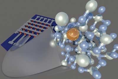 |
| This shows the study’s crossbar array design — vertical and horizontal electrodes with red memory cells where they intersect. “Flying out” of a single memory cell is a model of its molecular structure with tin (gold sphere) diffusing through the insulating HfO2 layer (blue and white matrix). Each component is essential in forming the filament across the metal-insulator-metal stack in this resistive switching architecture. (Image: Argonne National Laboratory) |
| Our appetite for data demands cheap, fast, nonvolatile, energy-efficient and scalable solid-state memory. One such type — called conductive bridge random access memory — has the promise to fit these requirements. |
| A memory device of this kind stacks three layers one upon another — metal, insulator and metal. In its off state, the insulator prevents conduction of electrons from the first metal, the anode, to the second metal, the cathode. In its on state, triggered by an external voltage, the insulator drops its resistance due to formation of a metallic bridge composed of cations (positively charged ions) from the anode and allows electron conduction from the first to the second metal. The cationic bridge remains embedded in the insulator and stores a unit of information until the voltage reverses. When reversed, the voltage dissolves the bridge and deletes the information, returning the memory to its original state. |
| Silver or copper typically held the role of bridge-builders. These metals can build bridges — or extend filaments — because they diffuse quickly. The disadvantage is that they diffuse quickly into silicon and contaminate surrounding silicon circuitry. To fix this problem, manufacturers separate the devices with barriers or liners, which increases production cost of the solid-state memory. |
| As it turns out, tin diffuses fast enough to form extended filaments, a characteristic found by Sushant Sonde, a resident associate in Argonne’s Nanoscience and Technology division, and Supratik Guha, director of the Nanoscience and Technology division and the Center for Nanoscale Materials (CNM) — both have joint appointments with the University of Chicago’s Institute for Molecular Engineering where Guha is also a professor — and their research team. However, owing to its silicon-compatible chemical nature, tin does not contaminate silicon. |
| Silicon and tin belong to the same atomic group. They have the same number of electrons in their outer shell and can form the same types of chemical bonds, whereas copper and silver belong to a different atomic group. |
| “Tin’s isovalent with silicon, together with its slower diffusion rate in silicon, compared to silver and copper, offers the flexibility to design systems compatible with semiconductor technology used in today’s industry,” explained Sonde. |
| How did the researchers know tin would perform so well in this role? |
| First, assisted by CNM scientist Subramanian Sankaranarayanan, they created a predictive framework to calculate the diffusion rates of different metals in the insulating layer through the use of Carbon, CNM’s high-performance computing cluster. The results validated silver and copper’s performance and predicted tin’s performance. The team’s new framework not only justifies the choice of standard electrode metals (silver and copper) but also allows exploration of other candidate metals. |
| Next, they made test structures with tin, silver and copper in a 3-D “crossbar” architecture in a semiconductor fabrication cleanroom at the CNM. This architecture allows for 3-D devices since the structure is layered upward, not outward, thus conserving space. |
| The team compared how silver, copper and tin performed in the new devices using the CNM’s characterization tools including a new ultrafast semiconductor parameter analyzer, a variable temperature electrical probe station and electron microscopy and X-ray techniques. |
| Compared to standard materials, tin performed as well for speed and favorably for stability under high thermal stress. The tin electrode enables the high thermal functionality, bearing out the framework’s prediction of best-performing electrode metals. |
| “This agreement is promising for future application of the framework,” said Sonde. “We may be able to fine tune memory device performance or find newer functionality based on our criterion.” |
| The team studied how a filament evolves over time and measured how long a filament takes to form. This rare peek into the inner workings of a memory device revealed that critical time depends not only on type of metal but also on differences in local microstructure. |
| Source: Argonne National Laboratory |
|
Subscribe to a free copy of one of our daily Nanowerk Newsletter Email Digests with a compilation of all of the day's news. |

