| Aug 15, 2018 |
Designing nanocrystals for more efficient optoelectronics(Nanowerk News) New artificial materials for semiconductors used in solar cells or photoelectrochemical cells that are designed from scratch with totally new and tailored properties: this is the latest research topic of Stefan Wippermann, head of the group “Atomistic Modelling“ at the Max-Planck-Institut für Eisenforschung), and his team. They characterized for the first time with atomic resolution a typical material system and are able to set design principles. |
| Their work introduces a new class of nanocrystal-in-glass systems, which increase the efficiency of optoelectronics such as photovoltaics and light-induced water splitting. |
| The Max Planck researchers published their latest findings in the journal Nature Nanotechnology ("Surface chemistry and buried interfaces in all-inorganic nanocrystalline solids"). |
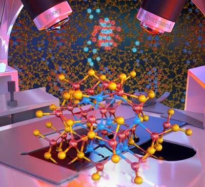 |
| The luminescent atoms in the image show a nanocrystal which is characterized with atomistic resolution, including its interface chemistry. (Image: Peter Allen) |
| Nanocrystals can be used as “artificial atoms” to create designer materials for electronic applications and solar energy conversion as they are controllable, potentially non-toxic and earth-abundant. In collaboration with the groups of Dmitri Talapin and Giulia Galli, University of Chicago, wet-chemical techniques were used to synthesize those nanocrystals and assemble them into semiconducting nanocomposites. |
| “One great advantage of designing nanocrystals is that we are able to choose their properties”, explains Wippermann. “As we develop our own “atoms”, we do not rely anymore on the chemical properties of elements but are able to design materials with target properties through nanostructuring.” |
| That means the researchers can abstain for example from toxic or rare elements. And even though their current model system is still using toxic elements, they embed the nanocrystals into solid matrices so that the nanocrystals are not spread into air. |
| “The current key challenge is not the production of the nanocrystals themselves but rather the understanding and controlling of their interface chemistry and defects, as their surfaces and interfaces are only a few nanometres in size and buried inside the material”, says Wippermann. |
| He and his team produced and analysed buried interfaces in solids of indium arsenide nanoparticles capped with thiostannate (Sn2S64-) ligands as prototypical nanocomposites. The ligands are used during the synthesis of the nanocomposites. With the help of theoretical and experimental techniques they found that the ligands are not adsorbed as intact units but decompose upon contact with the nanocrystal surface, forming an amorphous matrix around the nanocrystals. |
| Exactly this matrix influences the electronic transport of the nanocrystal solids, as the decomposed ligands form a passivation layer on the nanocrystal surface and only on top of this layer an intact ligand may adsorb. |
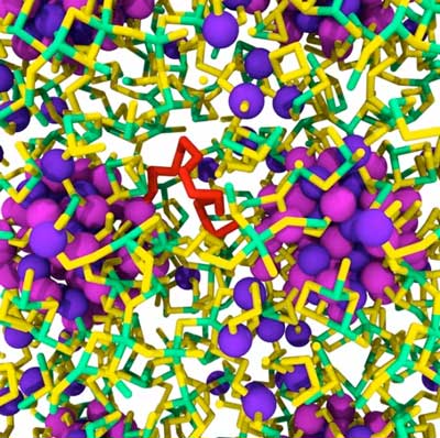 |
| Indium arsenide nanocrystals embedded in amorphous SnS3. Magenta and violet balls, green and yellow tubes denote indium, arsenic, tin and sulphur atoms, respectively. A sulphur chain in red. (Image: Stefan Wippermann) |
| Another passivation mechanism is the incorporation of sulphur into the subsurface layer. Arsenic in turn diffuses into the matrix, leading to the formation of characteristic defects. These defects explain the observed switching between positive and negative photoconductivity. Simulations showed that the indium arsenide nanocrystals draw sulphur from the matrix leading to the formation of a sulphur shell around the nanocrystals. |
| Sulphur also affects the amount and character of defects in the nanocomposite: A high sulphur content reduces the number of dangling bond defects in the nanocomposite and leads to the formation of sulphur chains acting as hole-conducting interconnects between the nanocrystals. |
| The Max Planck scientists show that the properties of nanocrystal-based solids are influenced by the size, shape, composition, surface chemistry and mutual interactions of nanocrystals. The strong quantum confinement of charge carriers inside the nanocrystals enable efficient carrier multiplication, where a single high energy photon creates multiple electron-hole pairs, which contribute to the conductivity. |
| This way optoelectronics can be made more efficient. Nanocrystals capped with molecular metal chalcogenide complexes have especially high electron mobilities, which allow for fast extraction of the photogenerated charges. The scientists established a strategy to characterize buried interfaces in inorganic nanocomposites and more generally nanoparticle-in-glass systems. |
| This strategy will help in designing tailor-made nanomaterials. The researchers now suggests to employ the presented strategy to technologically relevant semiconductor nanocomposites and nanoparticle-in-glass systems. |
| Source: Max-Planck-Institut für Eisenforschung |
|
Subscribe to a free copy of one of our daily Nanowerk Newsletter Email Digests with a compilation of all of the day's news. |

