| Posted: Sep 26, 2018 |
Oxygen vs. nanochip: Scientists show vulnerability of a promising 2D semiconductor to air(Nanowerk News) For the first time ever, an international team of scientists from NUST MISIS, the Hungarian Academy of Sciences, the University of Namur (Belgium), and Korea Research Institute for Standards & Science has managed to trace in details the structural changes of two-dimensional molybdenum disulfide under long-term environmental impact. The new data narrows the scope of its potential application in microelectronics and at the same time opens up new prospects for the use of two-dimensional materials as catalysts. |
| The research results have been published in the international scientific journal Nature Chemistry ("Spontaneous doping of the basal plane of MoS2 single layers through oxygen substitution under ambient conditions"). |
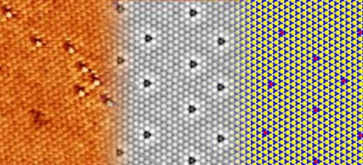 |
| Left - an experimental image of MoS2 with defects resulting from environmental exposure (obtained by scanning tunneling microscope STM), middle – the results of the simulation of the STM image, right – the model of the layer’s atomic structure. (Image: NUST MiSiS) |
| Molybdenum disulfide (MoS2) is considered a promising basis for a variety of ultra-small electronic devices such as high-frequency detectors, rectifiers, and transistors, so research teams around the world are actively studying its two-dimensional format, nanofilm. However, the new research conducted by NUST MISIS scientists has demonstrated that when this two-dimensional material is significantly oxidized in air, it turns into another connection. |
| Any electronic device using MoS2, without proper protection would simply stop working relatively quickly. To potentially use MoS2 in microelectronics, the devices would have to be encapsulated. |
| "For the first time ever, we have managed to experimentally prove that a single-layer molybdenum disulfide strongly degrades under environmental conditions, oxidizing and turning into a solid solution MoS2-xOx. The functions of a two-dimensional semiconductor without defects and losses can be implemented with molybdenum diselenides, another material with a similar structure," said Pavel Sorokin, head of the research team and leading researcher at the NUST MISIS Laboratory of Inorganic Nanomaterials. |
| In the experiments, two-dimensional layers of molybdenum disulfide obtained as a result of the stratification of molybdenum disulfide crystals by ultrasound, were maintained in environmental conditions at normal room temperature and lighting for long periods (more than a year and a half), during which scientists observed the changes in the structure of its surface. |
| "Thanks to the use of tunneling microscopy, we were able to track the structural changes of crystals of two-dimensional sulfur disulfide at the atomic level during long-term exposure to environmental conditions. We have discovered that the material previously considered stable is actually subject to spontaneous oxidation, but at the same time, the original crystal structure of MoS2 monolayers retains formations of MoS2-xOx solid solutions. Our simulations have allowed us to propose a mechanism of forming such solid solutions, and the results of the theoretical calculations are in complete agreement with our experimental measurements" - said Zakhar Popov, one of the co-authors of the study and a senior researcher at the NUST MISIS Laboratory of Inorganic Nanomaterials. |
| "The study's second key discovery is the new material that the monolayer of the molybdenum disulfide turns into is a two-dimensional crystal of a solid solution MoS2-xOx, which is an effective catalyst for electromechanical processes", concluded Sorokin. |
| Source: The National University of Science and Technology MISiS |
|
Subscribe to a free copy of one of our daily Nanowerk Newsletter Email Digests with a compilation of all of the day's news. |

