| Posted: Oct 03, 2018 |
Revolutionary ultra-thin metalens enables full-color imaging(Nanowerk News) Light of different colors travels at different speeds in different materials and structures. This is why we see white light split into its constituent colors after refracting through a prism, a phenomenon called dispersion. An ordinary lens cannot focus light of different colors to a single spot due to dispersion. This means different colors are never in focus at the same time, and so an image formed by such a simple lens is inevitably blurred. Conventional imaging systems solve this problem by stacking multiple lenses, but this solution comes at the cost of increased complexity and weight. |
| Columbia Engineering researchers have created the first flat lens capable of correctly focusing a large range of colors of any polarization to the same focal spot without the need for any additional elements. Only a micron thick, their revolutionary "flat" lens is much thinner than a sheet of paper and offers performance comparable to top-of-the-line compound lens systems. |
| The findings of the team, led by Nanfang Yu, associate professor of applied physics, are outlined in a new study, published by Light: Science & Applications. |
| Broadband imaging in the near-infrared using a single meta-lens, showing the ability of the lens in correcting chromatic aberrations, and manufacturing of meta-lenses using planar fabrication techniques similar to those used in the integrated circuits industry. |
| A conventional lens works by routing all the light falling upon it through different paths so that the whole light wave arrives at the focal point at the same time. It is manufactured to do so by adding an increasing amount of delay to the light as it goes from the edge to the center of the lens. This is why a conventional lens is thicker at its center than at its edge. |
| With the goal of inventing a thinner, lighter, and cheaper lens, Yu’s team took a different approach. Using their expertise in optical “metasurfaces”—engineered two-dimensional structures—to control light propagation in free space, the researchers built flat lenses made of pixels, or “meta-atoms.” |
| Each meta-atom has a size that is just a fraction of the wavelength of light and delays the light passing through it by a different amount. By patterning a very thin flat layer of nanostructures on a substrate as thin as a human hair, the researchers were able to achieve the same function as a much thicker and heavier conventional lens system. |
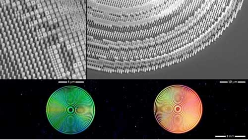 |
| Fig.1 Top panels: Scanning electron micrographs of sections of broadband meta-lenses. They are composed of silicon nanopillars with various cross-sectional shapes patterned on a glass substrate. Bottom panel: Photo showing two elements of a multi-element meta-lens imaging system. (Image: Sajan Shrestha, Adam Overvig, Nanfang Yu/Columbia Engineering) |
| Looking to the future, they anticipate that the meta-lenses could replace bulky lens systems, comparable to the way flat-screen TVs have replaced cathode-ray-tube TVs. |
| “The beauty of our flat lens is that by using meta-atoms of complex shapes, it not only provides the correct distribution of delay for a single color of light but also for a continuous spectrum of light,” Yu says. “And because they are so thin, they have the potential to drastically reduce the size and weight of any optical instrument or device used for imaging, such as cameras, microscopes, telescopes, and even our eyeglasses. Think of a pair of eyeglasses with a thickness thinner than a sheet of paper, smartphone cameras that do not bulge out, thin patches of imaging and sensing systems for driverless cars and drones, and miniaturized tools for medical imaging applications.” |
| Yu’s team fabricated the meta-lenses using standard 2D planar fabrication techniques similar to those used for fabricating computer chips. They say the process of mass manufacturing meta-lenses should be a good deal simpler than producing computer chips, as they need to define just one layer of nanostructures—in comparison, modern computer chips need numerous layers, some as many as 100. The advantage of the flat meta-lenses is that, unlike conventional lenses, they do not need to go through the costly and time-consuming grinding and polishing processes. |
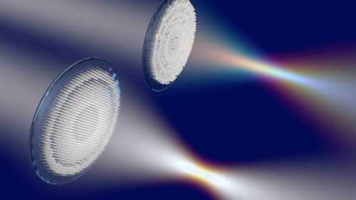 |
| Fig. 2 Illustration showing a comparison between two types of flat lenses. In the foreground, a new type of flat lens focuses all colors of light to the same spot. As a comparison, the flat lens in the background is not color-corrected. (Image: Adam Overvig/ Columbia Engineering ) |
| “The production of our flat lenses can be massively parallelized, yielding large quantities of high performance and cheap lenses,” notes Sajan Shrestha, a doctoral student in Yu’s group who was co-lead author of the study. “We can therefore send our lens designs to semiconductor foundries for mass production and benefit from economies of scale inherent in the industry.” |
| Because the flat lens can focus light with wavelengths ranging from 1.2 to 1.7 microns in the near-infrared to the same focal spot, it can form “colorful” images in the near-infrared band because all of the colors are in focus at the same time—essential for color photography. The lens can focus light of any arbitrary polarization state, so that it works not only in a lab setting, where the polarization can be well controlled, but also in real world applications, where ambient light has random polarization. It also works for transmitted light, convenient for integration into an optical system. |
| “Our design algorithm exhausts all degrees of freedom in sculpting an interface into a binary pattern, and, as a result, our flat lenses are able to reach performance approaching the theoretic limit that a single nanostructured interface can possibly achieve,” Adam Overvig, the study’s other co-lead author and also a doctoral student with Yu, says. “In fact, we’ve demonstrated a few flat lenses with the best theoretically possible combined traits: for a given meta-lens diameter, we have achieved the tightest focal spot over the largest wavelength range.” |
| Adds University of Pennsylvania H. Nedwill Ramsey Professor Nader Engheta, an expert in nanophotonics and metamaterials who was not involved with this study: "This is an elegant work from Professor Nanfang Yu’s group and it is an exciting development in the field of flat optics. This achromatic meta-lens, which is the state-of-the-art in engineering of metasurfaces, can open doors to new innovations in a diverse set of applications involving imaging, sensing, and compact camera technology.” |
| Now that the meta-lenses built by Yu and his colleagues are approaching the performance of high-quality imaging lens sets, with much smaller weight and size, the team has another challenge: improving the lenses’ efficiency. The flat lenses currently are not optimal because a small fraction of the incident optical power is either reflected by the flat lens, or scattered into unwanted directions. |
| The team is optimistic that the issue of efficiency is not fundamental, and they are busy inventing new design strategies to address the efficiency problem. They are also in talks with industry on further developing and licensing the technology. |
| Source: Columbia University School of Engineering and Applied Science |
|
Subscribe to a free copy of one of our daily Nanowerk Newsletter Email Digests with a compilation of all of the day's news. |

