| Posted: Oct 04, 2018 |
Extracting energy from a 60 nanometers thin layer(Nanowerk News) A team of researchers has demonstrated the viability of the direct piezoelectric effect in a thin film Bismuth Ferrite Material (BFO) for the first time (Nanoscale, "Direct and Converse Piezoelectric Responses at the Nanoscale from Epitaxial BiFeO3 Thin Films Grown by Polymer Assisted Deposition") |
| In this particular research, the BFO was scanned in a novel methodology called Direct Piezoelectric Force Microscopy (DPFM), a new AFM mode invented in 2017 (Nature Communications, "Piezo-generated charge mapping revealed through direct piezoelectric force microscopy"). |
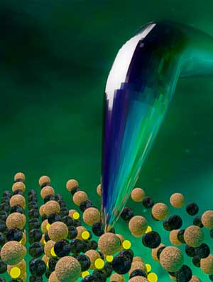 |
| Figure 1: 3D representation of the AFM nanometric tip used to obtain the direct piezoelectric characteristic of a thin film ferroelectric material. The BFO ferroelectric material, with perovskite crystal structure, was used to demonstrate that the direct effect takes a role at the nanoscale level. |
| The material in this mode is stressed by the AFM tip with nanometric size. The tip applies a force in the range of hundreds of microNewton and measures the generated charge that is created by the material. |
| For the case of BFO material, the piezoelectric characteristics were collected when the tip crosses antiparallel domain configurations, see the following video for a 3D representation of the tip crossing such configuration: |
| The good quality of the films arising from a novel method based in polymer assisted deposition ensured a constant and reliable current signal. Nevertheless the reliability, the signal to measure is, because of the generated charge, extremely weak. |
| Specifically, researcher measured currents in the femtoAmpere level (10E-15 Amperes). Consider that a typical personal computer consumes around 1 A. |
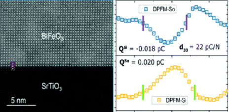 |
| Figure 2: STEM image obtained at the interface between the substrate and the BFO with excellent quality and current lines obtained in DPFM that were used to obtain the piezoelectric characteristics of the films. |
| The current signal was integrated to find the d33 characteristics of the material. This research is crucial for the development of piezoelectric material and it is understanding at the nanoscale, being the very first time that the direct piezoelectric effect also works at the nanoscale. |
| Source: ICMAB |
|
Subscribe to a free copy of one of our daily Nanowerk Newsletter Email Digests with a compilation of all of the day's news. |

