| Posted: Oct 04, 2018 |
Making a movie of nanocrystals' structural evolution(Nanowerk News) When you rapidly turn the pages of a flipbook, the series of static images look like they are moving. Scientists recently applied a similar principle to capture how the structure of a material changes over extremely short time scales – mere trillionths of a second or faster. To record this atomic-scale motion, they needed a special instrument housed at the U.S. Department of Energy’s (DOE) Brookhaven National Laboratory. |
| “This ultrafast electron difraction instrument, which has electron beams with an energy of one million electron volts, was designed and made in house,” said Jing Tao, a physicist in Brookhaven Lab’s Condensed Matter Physics and Materials Science (CMPMS) Department and corresponding author on the Applied Physics Letters paper reporting the work ("Probing the pathway of an ultrafast structural phase transition to illuminate the transition mechanism in Cu2S"). “We collaborated with the Lab’s Accelerator Test Facility to ensure that temperature, humidity, and other environmental conditions remained stable and that the instrument was properly aligned.” |
| A movie of the nanocrystals' structural evolution (schematic) in real space, as noted by the change in intensity of the rings. |
| Today’s electron microscopes can resolve single atoms, but typically only at exposure times on the order of seconds. However, atoms move much more quickly than that. |
| “We are looking at structural dynamics that happen within hundreds of femtoseconds to a few picoseconds,” said first author Junjie Li, a physicist in the CMPMS Department. “For reference, one femtosecond is equivalent to one quadrillionth of a second.” |
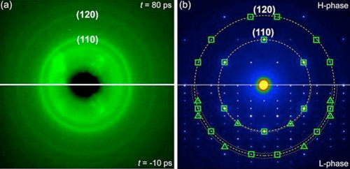 |
| The scientists obtained ultrafast electron diffraction (UED) patterns before and after they excited the copper sulfide sample with laser pulses ((a), bottom and top images, respectively). The (110) and (120) refer to different surfaces, or planes, of the sample. The scientists also obtained electron diffraction patterns of the material's monoclinic, or low-symmetry, phase and its high-symmetry hexagonal phase through transmission electron microscopy ((b), bottom and top images, respectively). The open squares represent diffraction peaks that appear in both phases, while the open triangles represent peaks that only appear in the low-symmetry phase. (Image: Brookhaven National Laboratory) |
| In this study, the scientists probed the structure of copper sulfide nanocrystals. Above a certain temperature, copper sulfide undergoes a transition in which its crystal structure changes from a low-symmetry to a high-symmetry phase. During this phase transition, its copper ions become highly mobile, making it a promising material for next-generation electrochemical and thermoelectric devices, such as batteries and electrical switches. |
| “All material properties have a structural origin,” said Tao. “Identifying and understanding the mechanism that is driving a material’s structure is key to improving its performance for real-world applications.” |
| The optimal properties of materials often emerge at phase transitions involving simultaneous changes in crystal symmetry, electronic structure, and magnetic susceptibility, making it difficult to determine the primary force driving the transition. |
| Previous experiments conducted by other groups demonstrated that the structural phase transition in copper sulfide was caused by a diffusion of copper ions. Then, the Brookhaven team discovered that continually increasing or decreasing the number of electrons pumped into the material over time caused its crystal structure to oscillate between the low- and high-symmetry phases at room temperature (PNAS, "Reversible structure manipulation by tuning carrier concentration in metastable Cu2S"). |
| “We were surprised to find that a minimal change in the electron dose rate brings about a huge collective movement of the copper ions because it showed that the structural phase transition is somehow related to electronic manipulation,” said Tao. “We knew there must be an intrinsic relationship, but had no proof. The femtosecond time resolution provided by our instrument made it possible for us to see how the movement of the copper ions is correlated with changes in electronic structure.” |
| To initiate the structural transition, the scientists “pumped” the material with laser pulses, bringing it into its excited energy state. After well-controlled time delays, they then sent electron pulses through the sample and recorded the way in which the electrons were scattered. The resulting electron diffraction patterns revealed the crystal structure of the material at the exact moments that the electron beam interacted with it. |
| By combining these structural “snapshots” taken at various time delays between the laser and electron pulses, they produced a movie capturing the way that the structure evolves from the beginning to the end of the phase transition. |
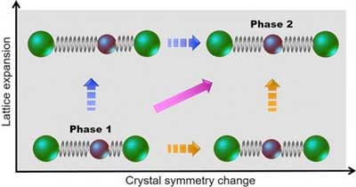 |
| A material can take multiple pathways when transforming from one phase to another. This schematic shows a structural phase transition for a one-dimensional assembly of atoms in which the symmetry of the crystal breaks and the lattice expands. Right before the laser pulse arrives (phase 1), there are two types of atoms (green and brown circles) that are unequally spaced. The pulse drives the material from phase 1 to 2, in which the atom types are the same but the lattice symmetry and spacing are different. The orange, magenta, and blue arrows indicate the possible transition pathways in the ultrafast time domain. (Image: Brookhaven National Laboratory) |
| In analyzing the electron diffraction signatures, Li was shocked to discover that the structural phase transition involved two separate processes that took place on very different time scales. |
| “I found that the crystal symmetry, or how the ions arrange themselves, breaks in two picoseconds, and the volume of the crystal lattice expands from 10 to 20 picoseconds,” said Li. “Up until now, scientists had thought that the symmetry and volume changed at the same time. Because of insufficient time resolution, they were only able to take one snapshot at the beginning of the transition and another one at the end and thus did not capture what was happening in between.” |
| It turns out that the time scale of the crystal symmetry change coincides with that of another process: electronic carrier relaxation, or the movement of electrons from an excited energy state (induced by the laser excitation) to the ground state. Given this coincidence, the Brookhaven team believes that interactions between the electrons and atoms vibrating in the lattice (phonons) could be behind the crystal symmetry transition. |
| “The fact that both processes happen at two picoseconds strongly suggests that electron-phonon coupling governs the transition,” said Li. “Scientists think electron-phonon coupling plays a very important role in many strongly correlated and quantum materials with emergent properties—for example, superconductors, which can carry electricity without resistance, and multiferroics, which exhibit spontaneous magnetic and electric polarizations. But this mechanism is still not entirely understood, even after decades of research.” |
| Now that the scientists have the proper equipment to capture ultrafast structural dynamics, they hope to find the origin of phase transitions in other materials. |
| “The scientific community took for granted that the crystal symmetry breaking and lattice expansion occur together,” said Tao. “The ability to separate these processes is a breakthrough that will help us understand structure-property relationships in a wide range of materials.” |
| Source: Brookhaven National Laboratory |
|
Subscribe to a free copy of one of our daily Nanowerk Newsletter Email Digests with a compilation of all of the day's news. |

