| Posted: Oct 12, 2018 | |
Light switch: Scientists develop method to control nanoscale manipulation in scanning tunneling microscopes(Nanowerk News) Researchers from Japan have taken a step toward faster and more advanced electronics by developing a way to better measure and manipulate conductive materials through scanning tunneling microscopy. |
|
| The team published their results in July in Nano Letters ("Tailoring Single-Cycle Near Field in a Tunnel Junction with Carrier-Envelope Phase-Controlled Terahertz Electric Fields"), an American Chemical Society journal. Scientists from the University of Tokyo, Yokohama National University, and the Central Research Laboratory of Hamamatsu Photonics contributed to this paper. | |
 |
|
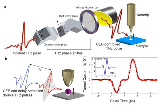
| (a) Schematic of phase-controlled THz-STM. (b) Ultrafast current burst induced by phase-controlled and delay-controlled double THz near-fields. A sinusoidal THz near field produces ultrafast bidirectional current burst between a sample and a nanotip. By precisely tuning the carrier envelope phase (CEP) of THz near field, the direction and the timing of the current burst can be desirably manipulated on the femotosecond timescale. (Image: Yokohama National University) (click on image to enlarge) | |
| Scanning tunneling microscopy (STM) involves placing a conducting tip close to the surface of the conductive material to be imaged. A voltage is applied through the tip to the surface, creating a "tunnel junction" between the two through which electrons travel. | |
| The shape and position of the tip, the voltage strength, and the conductivity and density of the material's surface all come together to provide the scientist with a better understanding of the atomic structure of the material being imaged. With that information, the scientist should be able to change the variables to manipulate the material itself. | |
| Precise manipulation, however, has been a problem - until now. | |
| The researchers designed a custom terahertz pulse cycle that quickly oscillates between near and far fields within the desired electrical current. | |
| "The characterization and active control of near fields in a tunnel junction are essential for advancing elaborate manipulation of light-field-driven processes at the nanoscale," said Jun Takeda, a professor in the department of physics in the Graduate School of Engineering at Yokohama National University. "We demonstrated that desirable phase-controlled near fields can be produced in a tunnel junction via terahertz scanning tunneling microscopy with a phase shifter." | |
| According to Takeda, previous studies in this area assumed that the near and far fields were the same - spatially and temporally. His team examined the fields closely and not only identified that there was a difference between the two, but realized that the pulse of fast laser could prompt the needed phase shift of the terahertz pulse to switch the current to the near field. | |
| "Our work holds enormous promise for advancing strong-field physics in nano-scale solid state systems, such as the phase change materials used for optical storage media in DVDs and Blu-ray, as well as next-generation ultrafast electronics and microscopies," Takeda said. |
| Source: Yokohama National University | |
|
Subscribe to a free copy of one of our daily Nanowerk Newsletter Email Digests with a compilation of all of the day's news. |
