| Posted: Oct 17, 2018 |
On the way to new electronic materials with metal-organic networks(Nanowerk News) Scientists at the Max Planck Institute for Polymer Research (MPI-P) in Mainz (Germany) together with scientists from Dresden, Leipzig, Sofia (Bulgaria) and Madrid (Spain) have now developed and characterized a novel, metal-organic material which displays electrical properties mimicking those of highly crystalline silicon. The material which can easily be fabricated at room temperature could serve as a replacement for expensive conventional inorganic materials used in optoelectronics ("High-mobility band-like charge transport in a semiconducting two-dimensional metal–organic framework"). |
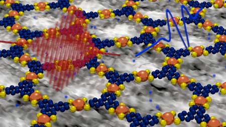 |
| A metal-organic framework could serve as a replacement for the semiconductor silicon in the future. (Image: MPI-P) |
| Silicon, a so called semiconductor, is currently widely employed for the development of components such as solar cells, LEDs or computer chips. High purity silicon, a highly ordered material which is expensive to produce, is required to develop such applications. This is due to the fact that the electrical properties of a semiconductor (as silicon) are strongly affected by disorder. |
| The scientists around group leader Enrique Cánovas (MPI-P, Department of Prof. Dr. Mischa Bonn) have now developed a novel low cost metal-organic framework (MOF), which has similar electrical properties. |
| The MOF, produced by Xinliang Feng´s group in Dresden, is a highly crystalline solid made of iron ions linked by organic molecules, hence the name metal-organic framework. In contrast to silicon, the material can be made at room temperature, and the sample chemistry, morphology and electronic properties are easily customizable during the manufacturing process. |
| MOFs produced in the past showed no or very little electrical conductivity, this prevented MOFs to be employed in optoelectronic applications, where an “easy” displacement of electrons under an applied electrical field is required. With the novel MOF, the researchers from Mainz have now demonstrated - for an organic-based material - a behavior of the conductivity similar to silicon, a so-called "Drude behavior" (named after the physicist Paul Drude). |
| A Drude behavior implies that electrons within the material are almost free to move under the application of an external electric field, i.e. if a voltage is applied. This behavior, a common observable for highly ordered inorganic crystals like silicon, has been hardly seen in organic based materials; organic based materials are generally disordered in nature, unlike MOFs. |
| To characterize the unique properties for the developed MOF, the scientists at MPI-P employed ultrafast terahertz spectroscopy, a tool that allows measuring the conductivity of the material without requiring physical – perturbative - contacts. |
| Using this tool, energy is transferred to the electrons in the semicondcuting material due to the absorption of light (mediated by an ultrafast laser pump pulse in the visible region). |
| A second laser pulse - a so-called terahertz probe, which oscillates about a factor of 1000 slower than visible light – allows to interrogate the conductivity for the photo-generated electrons. This results in a frequency dependent conductivity signal from which the scientists were able to model by “Drude” the nature of the transport of the electrons in the MOF. |
| “From this response, we obtained record mobilities of the electrons in such materials which exceed the mobilities measured in insulating MOFs by a factor of 10000”, says Dr. Enrique Canovas of the MPI-P. This means that electrons can easily drift under an electric field over long distances in MOFs, an aspect that was independently verified in ~1000 micron length devices. Thus, the new material paves the way for the use of MOFs in optoelectronics. |
| In the future, the researchers will work on the ability to directly set and predict the electronic properties via tuning the composition of their produced metal-organic framework. |
| Source: Max Planck Institute for Polymer Research |
|
Subscribe to a free copy of one of our daily Nanowerk Newsletter Email Digests with a compilation of all of the day's news. |

