| Oct 26, 2018 |
Nanocrystals arrange to improve electronics(Nanowerk News) Lawrence Livermore National Laboratory (LLNL) researchers are working to make better electronic devices by delving into the way nanocrystals are arranged inside of them. |
| Nanocrystals are promising building blocks for new and improved electronic devices, due to their size-tunable properties and ability to integrate into devices at low-cost. |
| While the structure of nanocrystals has been extensively studied, no one has been able to watch the full assembly process. |
| That’s where LLNL scientists Christine Orme, Yixuan Yu, Babak Sadigh and a colleague from the University of California, Los Angeles come in. |
| ‘We think the situation can be improved if detailed quantitative information on the nanocrystal assembly process could be identified and if the crystallization process were better controlled,” said Orme, an LLNL material scientist and corresponding author of a paper appearing in the journal Nature Communications ("Space- and time-resolved small angle X-ray scattering to probe assembly of silver nanocrystal superlattices"). |
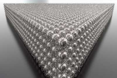 |
| Electric fields assemble silver nanocrystals into a superlattice. (Image: Jacob Long/LLNL) |
| Nanocrystals inside devices form ensembles, whose collective physical properties, such as charge carrier mobility, depend on both the properties of individual nanocrystals and the way they are arranged. In principle, ordered nanocrystal ensembles, or superlattices, allow for more control in charge transport by facilitating the formation of minibands. However, in practice, few devices built from ordered nanocrystal superlattices are on the market. |
| Most previous studies use solution evaporation methods to generate nanocrystal superlattices and probe the assembly process as the solvent is being gradually removed. It is difficult to obtain quantitative information on the assembly process, however, because the volume and shape of the nanocrystal solution is continually changing in an uncontrollable manner and the capillary forces can drive nanocrystal motion during drying. |
| Electric field-driven growth offers a solution to this problem. “We have recently demonstrated that an electric field can be used to drive the assembly of well-ordered, 3D nanocrystal superlattices,” Orme said. |
| Because the electric field increases the local concentration without changing the volume, shape or composition of nanocrystal solution, the crystallizing system can be probed quantitatively without complications associated with capillary forces or scattering from drying interfaces. |
| As anticipated, the team found that the electric field drives nanocrystals toward the surface, creating a concentration gradient that leads to nucleation and growth of superlattices. Surprisingly, the field also sorts the particles according to size. In essence, the electric field both concentrates and purifies the nanocrystal solution during growth. |
| “Because of this size sorting effect, the superlattice crystals are better ordered and the size of the nanocrystals in the lattice can be tuned during growth,” Orme said. “This might be a useful tool for optoelectronic devices. We’re working on infrared detectors now and think it might be an interesting strategy for improving color in monitors.” |
| Source: Lawrence Livermore National Laboratory |
|
Subscribe to a free copy of one of our daily Nanowerk Newsletter Email Digests with a compilation of all of the day's news. |

