| Oct 26, 2018 |
Scientists form atomically flat tellurium(Nanowerk News) In the way things often happens in science, Amey Apte wasn’t looking for two-dimensional tellurium while experimenting with materials at Rice University. But there it was. |
| “It’s like I tried to find a penny and instead found a dollar,” he said. |
| Apte and his colleagues made tellurium, a rare metal, into a film less than a nanometer thick by melting a powder of the element at high temperature and blowing the atoms onto a surface. He said the resulting material, tellurene, shows promise for next-generation, near-infrared solar cells and other optoelectronic applications that rely on the manipulation of light. |
| The slim jackpot is described in 2D Materials ("Polytypism in ultra-thin tellurium"). |
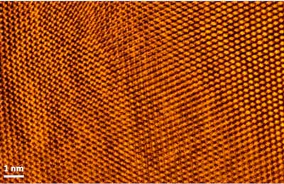 |
| Ripples in a lattice of tellurium atoms formed into three-layer tellurene at Rice University show several polytypes – different atomic arrangements based on how the layers are stacked – with distinct electronic and optical properties. (Image: Ajayan Research Group) |
| “I was trying to grow a transition metal dichalcogenide, tungsten ditelluride, but because tungsten has a high melting point it was difficult,” said Apte, a graduate student in the Rice lab of materials scientist Pulickel Ajayan and co-lead author of the paper. “But I observed some other films that caught my interest.” |
| The other films turned out to be ultrathin crystals of pure tellurium. Further experiments led the researchers to create the new material in two forms: A large, consistent film about 6 nanometers thick that covered a centimeter-square surface, and a three-atomic-layer film that measured less than a nanometer thick. |
| “Transition metal dichalcogenides are all the rage these days, but those are all compound 2D materials,” Ajayan said. “This material is a single element and shows as much structural richness and variety as a compound, so 2D tellurium is interesting from both a theoretical and experimental standpoint. Single element chalcogen layers of atomic thinness would be interesting but have not been studied much.” |
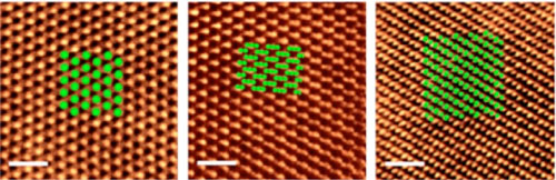 |
| Simulations of three-layer tellurene laid over a microscopic image of the material created at Rice University show the accuracy of how ripples in a sheet of the material would force the atoms into three distinct configurations. Though connected, these polytypes have different electronic and optical properties. (Image: Ajayan Research Group) |
| Images taken with Rice’s powerful electron microscope showed the atomic layers had arranged themselves precisely as theory predicted, as graphene-like hexagonal sheets slightly offset to one another. The tellurene, made in a 650-degree Celsius (1,202-degree Fahrenheit) furnace by melting bulk tellurium powder, also appeared to be gently buckled in a way that subtly changes the relationships between the atoms on each layer. |
| “Because of that, we see different polytypes, which means the crystal structure of the material remains the same but the atomic arrangement can differ based on how the layers are stacked,” Apte said. “In this case, the three polytypes we see under the microscope match theoretically predicted structures and have completely different lattice arrangements that give each phase different properties.” |
| “The in-plane anisotropy also means that the properties of optical absorption, transmission or electrical conductivity are going to be different in the two principal directions,” said Rice graduate student and co-lead author Elizabeth Bianco. “For instance, tellurene can show electrical conduction up to three orders of magnitude higher than molybdenum disulfide, and it would be useful in optoelectronics.” |
| Thicker tellurium films were also made under vacuum at room temperature via pulsed laser deposition, which blasted atoms from bulk and allowed them to form a stable film on a magnesium oxide surface. |
| Tellurene could have topological properties with potential benefits for spintronics and magneto-electronics. “Tellurium atoms are much heavier than carbon,” Apte said. “They show a phenomenon called spin-orbit coupling, which is very weak in lighter elements, and allows for much more exotic physics like topological phases and quantum effects.” |
| “The fascinating thing about tellurene that differentiates it from other 2D materials is its unique crystalline structure and high melting temperature,” said co-author Ajit Roy, materials scientist at the Air Force Research Laboratory at Wright-Patterson Air Force Base in Dayton, Ohio. “That enables us to expand the performance envelope of optoelectronics, thermoelectric and other thin film devices.” |
| Co-author Priya Vashishta, a professor of materials science at the University of Southern California, Los Angeles, said the research exemplifies how experiment and theory complement each other, a cornerstone of USC’s Materials Genome Innovation for Computational Software center, supported by the Department of Energy Office of Science’s Basic Energy Sciences. |
| Source: By Mike Williams, Rice University |
|
Subscribe to a free copy of one of our daily Nanowerk Newsletter Email Digests with a compilation of all of the day's news. |

