| Oct 26, 2018 |
Delivering pressure with an unconventional crystal interface(Nanowerk News) The use of pressure to alter semiconductor properties is showing increasing promise in applications such as high-performance infrared sensors and energy conversion devices. With a novel and unconventional crystal interface, researchers at Rensselaer Polytechnic Institute have enabled more powerful and dynamic tuning of the method, which they initially pioneered in 2015. |
| “A conventional way to introduce strain or pressure in a functional material is to grow such a material on a substrate which is similar to the film material in materials chemistry but dissimilar in lattice constant. In our work, we broke away from this conventional wisdom” said Jian Shi, an assistant professor of materials science and engineering at Rensselaer Polytechnic Institute. |
| The research is detailed in a recent edition of Science Advances ("Defect-engineered epitaxial VO2±δ in strain engineering of heterogeneous soft crystals"). |
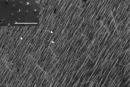 |
| Researchers deposited a dissimilar semiconductor material, halide perovskite, onto a defect engineered vanadium dioxide substrate. (Image: Rensselaer Polytechnic Institute) |
| Previous research using strain to alter semiconductor properties has focused on developing a coherent epitaxial interface between the film and substrate to transfer the strain from substrate to the film. For example, in elastic strain engineering, people grow germanium on silicon, oxides on oxides, chalcogenides on chalcogenides. |
| The Science Advances work introduces a new approach, depositing a dissimilar but technologically important semiconductor material – halide perovskite – onto a vanadium dioxide substrate. Halide perovskite has little impact on the chemistry of vanadium dioxide substrate. But when combined, the vanadium dioxide and halide perskovite form a heterogenous interface, which could allow strain to be effectively transferred to the semiconductor material. |
| The research uses a specially engineered substrate - vanadium dioxide - that is capable of a structural phase transition, meaning it changes structure under different temperatures. The researchers use the structural phase transition to impose strain on a thin film semiconductor deposited on its surface using chemical vapor deposition. |
| To enable large strain in the semiconductor layer, Yiping Wang, a graduate student in Shi’s lab, modified vanadium dioxide, adding and removing oxygen atoms from the material by controlling the partial pressure of oxygen during chemical vapor deposition of the vanadium dioxide as it is grown on a sapphire crystal. |
| The resulting “defect engineered” nanoforest arrays of vanadium dioxide have a large structural change under temperature stimulus, and can move through not one but three phase transitions, allowing them to more precisely tune the amount of pressure exerted on the semiconductor. |
| This unconventional approach, shows that the mechanical softness of the semiconductor crystals could be a key for the success of strain engineering. With a softer semiconductor, a moderate interface, and a more dynamic substrate, the researchers were able to dynamically modify the semiconductor’s physical properties in a reversible manner at the nanoscale. The pressure delivered was found large enough to trigger a structural and electronic phase transition in the semiconductor crystal. Such a transition in this crystal has been demonstrated under high pressure using a different but technologically impractical approach. |
| Source: Rensselaer Polytechnic Institute |
|
Subscribe to a free copy of one of our daily Nanowerk Newsletter Email Digests with a compilation of all of the day's news. |

