| Nov 16, 2018 |
Researchers study the reactions taking place in two-layer thin metal films(Nanowerk News) A team of researchers from Siberian Federal University (SFU) obtained thin copper/gold and iron/palladium films and studied the reactions that take place in them upon heating. Knowing these processes, scientists will be able to improve the properties of materials currently used in microelectronics. |
| The research was published in the Journal of Solid State Chemistry ("L10 ordered phase formation at solid state reactions in Cu/Au and Fe/Pd thin films"). |
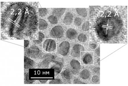 |
| This is an image of thin copper/gold film made with transmission electron microscope. |
| Materials based on thin metal films are widely used in microelectronics (e.g. copper and gold - in the manufacture of electrical contacts). Nanomaterials based on iron and palladium have unique magnetic properties and potentially can be used for high-density magnetic recording of information. |
| One of the main factors that affects the properties of thin film materials is alteration of the phase composition as a result of chemical reactions and atomic structure realignment. The work of the researchers covers solid phase reactions in two-layer thin metal films - copper/gold (Cu/Au) and iro/palladium (Fe/Pl). |
| The scientists obtained the Cu/Au and Fe/Pd films in SFU common use center. To do so, they used the method of electron-beam deposition in high vacuum, i.e. evaporated the alloy using a beam of electrons and then deposited it on a carrying base as a thin layer. The thickness of the layer could be regulated. After obtaining the films the scientists made an experiment to study the course of chemical reactions in the interface region of the initial elements. |
| For the reactions to take place, materials had to be heated to high temperatures which was done directly in the column of a transmission electron microscope. The team used a special sample holder that allowed for controlled heating of each sample from room temperature to 1,000°C. |
| Along with the heating, the team registered electron diffraction images and measured the temperature. Thus, the scientists managed to combine the initiation of the reaction and the registration of changes in a solid-phase reaction within one experiment and to secure high data precision. |
| "We've established the value of the long-range order parameter and the temperature of the order-disorder transition in atomically ordered phases formed in the course of the reaction. The atoms of such phases form ordered structures of certain shapes. We also suggested a mechanism for the formation of such ordered structures. For instance, in the case of the Cu/Au system we demonstrated how mutual diffusion of copper and gold on the initial stages of the reaction leads to the refinement of grains of the initial materials and the formation of Cu-Au solid solution nanocrystallites within the material. Later on, a new ordered structure occurs and starts to grow on the basis of these components," explains Evgeny Moiseenko, a co-author of the work, candidate of physics and mathematics, and a research assistant at SFU. |
| The work of the scientists will help identify the features of the studied thin film systems that may be used in the design of microelectronic devices. |
| Source: Siberian Federal University |
|
Subscribe to a free copy of one of our daily Nanowerk Newsletter Email Digests with a compilation of all of the day's news. |

