| Nov 19, 2018 |
Bending light around tight corners without backscattering losses(Nanowerk News) Engineers at Duke University have demonstrated a device that can direct photons of light around sharp corners with virtually no losses due to backscattering, a key property that will be needed if electronics are ever to be replaced by light-based devices. |
| The result was achieved with photonic crystals built on the concept of topological insulators, which won its discoverers a Nobel Prize in 2016. By carefully controlling the geometry of a crystal lattice, researchers can block light from traveling through its interior while transmitting it perfectly along its surface. |
| The device accomplishes its near-perfect transmittance around corners despite being much smaller than previous designs. |
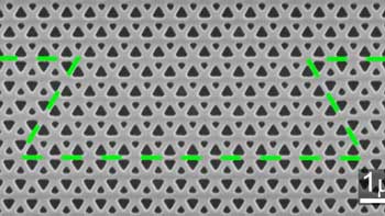 |
| The central part of the new photonic crystal topological insulator waveguide, with the path of a photon’s path highlighted in green. The experiment showed that each turn resulted in backscattering losses of only a few percent. |
| The Semiconductor Industry Association estimates that the number of electronic devices is increasing so rapidly that by the year 2040, there won’t be enough power in the entire world to run them all. One potential solution is to turn to massless photons to replace the electrons currently used for transmitting data. Besides saving energy, photonic systems also promise to be faster and have higher bandwidth. |
| Photons are already in use in some applications such as on-chip photonic communication. One drawback of the current technology, however, is that such systems cannot turn or bend light efficiently. But for photons to ever replace electrons in microchips, travelling around corners in microscopic spaces is a key. |
| “The smaller the device the better, but of course we’re trying to minimize losses as well,” said Wiktor Walasik, a postdoctoral associate in electrical and computer engineering at Duke. “There are a lot of people working to make an all-optical computing system possible. We’re not there yet, but I think that’s the direction we’re going.” |
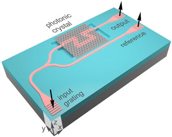 |
| A schematic of the new optical waveguide device showing the input and output gratings and silicon waveguide connections. |
| Previous demonstrations have also shown small losses while guiding photons around corners, but the new Duke research does it on a rectangular device just 35 micrometers long and 5.5 micrometers wide—100 times smaller than previously demonstrated ring-resonator-based devices. |
| In the new study, which appeared in the journal Nature Nanotechnology ("Robust Topologically Protected Transport In Photonic Crystals at Telecommunication Wavelengths"), researchers fabricated topological insulators using electron beam lithography and measured the light transmittance through a series of sharp turns. Each turn only resulted in the loss of a few percent. |
| “Guiding light around sharp corners in conventional photonic crystals was possible before but only through a long laborious process tailored to a specific set of parameters,” said Natasha Litchinitser, professor of electrical and computer engineering at Duke. “And if you made even the tiniest mistake in its fabrication, it lost a lot of the properties you were trying to optimize.” |
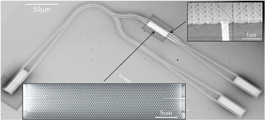 |
| A closer look at the new optical waveguide device featuring a zoomed-in view of the fabricated photonic crystal topological insulator. |
| “But our device will work no matter its dimensions or geometry of the photons’ path and photon transport is ‘topologically protected,’” added Mikhail Shalaev, a doctoral student in Litchinitser’s laboratory and first author of the paper. “This means that even if there are minor defects in the photonic crystalline structure, the waveguide still works very well. It is not so sensitive to fabrication errors.” |
| The researchers point out that their device also has a large operating bandwidth, is compatible with modern semiconductor fabrication technologies, and works at wavelengths currently used in telecommunications. |
| Now the researchers are trying to make a waveguide that can be turned on or off at will—another important feature for all-optical photon-based technologies to ever become a reality. |
| Source: By Ken Kingery, Duke University |
|
Subscribe to a free copy of one of our daily Nanowerk Newsletter Email Digests with a compilation of all of the day's news. |

