| Nov 30, 2018 |
Atomic nitrogen route to new 2D semiconductors(Nanowerk News) A simple and non-destructive fabrication technique could aid the manufacture of more energy efficient two-dimensional (2D) films needed to transform the electronics industry (ACS Nano, "Direct n- to p-type channel conversion in monolayer/few-layer WS2 field-effect transistors by atomic nitrogen treatment"). |
| Atomically thin, 2D transition metal dichalcogenides (TMDCs) like tungsten disulfide (WS2) exhibit remarkable physical, electronic and optoelectronic properties, such as flexibility, transparency and semi-conducting characteristics. |
| Although there has been significant progress in fabricating 2D TMDCs, the ultrathin nature of such 2D semiconductors precludes the usage of techniques like ion implantation, with subsequent activation annealing, for introducing and retaining dopants within mono- or few-layer TMDCs. |
| Now, Dongzhi Chi and colleagues from the Institute of Materials Research and Engineering and the Institute of High Performance Computing at A*STAR, in collaboration with researchers from the National University of Singapore, have developed an innovative technique that uses highly reactive nitrogen (N) atoms for controlling dopants within films of WS2 at the atomic scale, and promises a reliable method for doping 2D TMDCs. |
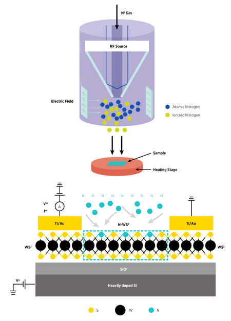 |
| (Top) Schematic of the atomic nitrogen generation process with a RF plasma. (Bottom) Cross-sectional view of bottom-gated monolayer and few-layer WS2 FETs with Ti/Au contacts. (© ACS) |
| “[The current] inability to effectively dope 2D TMDCs hinders developing energy efficient devices like field-effect transistors using manufacturing technologies currently employed in the semiconductor industry,” says Chi. |
| TMDCs like WS2 are typically n-type semiconductors and there are currently no reliable methods for making atomically-thin TMDCs that are p-type. This is particularly vexing as it means that 2D TMDC devices, by necessity, are mostly based on n-type CMOS-FETs — field-effect transistors (FETs) fabricated using complementary metal-oxide-semiconductor (CMOS) technologies. The lack of an effective way to make p-type 2D TMDC-based CMOS-FETs limits the creation of next generation electronics, optoelectronic devices, and clean energy technologies. |
| So the researchers looked to atomic nitrogen as unlike current doping techniques, such as ion-implantation or plasma implantation, it can produce effective p-type doping in 2D TMDC-based CMOS-FETs without causing noticeable structural damage. |
| To produce atomic N, they used a plasma to generate ionized and atomic N in a ceramic cavity and applied an electrical field to retain the nitrogen ions, allowing the N atoms to react with a sample of WS2 heated to 300 degrees C. |
| The high chemical activity and low kinetic energy of the N introduced modifications to the structure at mono- or few-layer depth in the WS2 by replacing sulfur atoms and forming W-N chemical bonds. This proved to be ideal for controlling the dopants at the atomic scale. |
| “Unlike other doping methods for TMDCs —such as molecular chemisorption, physisorption and nitrogen plasma doping — our method introduces nitrogen into substitutional sites of sulfur by replacing the sulfur with nitrogen, without causing damage to the TMDC layers,” says Chi. |
| “Our work could help to accelerate the development of next generation electronics and optoelectronics technologies, such as ultralow power logic circuits and smart sensors, based on 2D semiconducting TMDCs,” says Chi. |
| Source: A*STAR |
|
Subscribe to a free copy of one of our daily Nanowerk Newsletter Email Digests with a compilation of all of the day's news. |

