| Dec 06, 2018 |
Form-fitting, nanoscale sensors now make sense(Nanowerk News) What if a sensor sensing a thing could be part of the thing itself? Rice University engineers believe they have a two-dimensional solution to do just that. |
| Rice engineers led by materials scientists Pulickel Ajayan and Jun Lou have developed a method to make atom-flat sensors that seamlessly integrate with devices to report on what they perceive. |
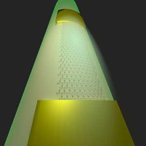 |
| Rice engineers have developed a method to transfer complete, flexible, two-dimensional circuits from their fabrication platforms to curved and other smooth surfaces. Such circuits are able to couple with near-field electromagnetic waves and offer next-generation sensing for optical fibers and other applications. (Illustration by Zehua Jin) |
| Electronically active 2D materials have been the subject of much research since the introduction of graphene in 2004. Even though they are often touted for their strength, they’re difficult to move to where they’re needed without destroying them. |
| The Ajayan and Lou groups, along with the lab of Rice engineer Jacob Robinson, have a new way to keep the materials and their associated circuitry, including electrodes, intact as they’re moved to curved or other smooth surfaces. |
| The results of their work appear in the American Chemical Society journal ACS Nano("Near-Field Coupled Integrable Two-Dimensional InSe Photosensor on Optical Fiber"). |
| The Rice team tested the concept by making a 10-nanometer-thick indium selenide photodetector with gold electrodes and placing it onto an optical fiber. Because it was so close, the near-field sensor effectively coupled with an evanescent field – the oscillating electromagnetic wave that rides the surface of the fiber – and accurately detected the flow of information inside. |
| The benefit is that these sensors can now be imbedded into such fibers where they can monitor performance without adding weight or hindering the signal flow. |
| “This paper proposes several interesting possibilities for applying 2D devices in real applications,” Lou said. “For example, optical fibers at the bottom of the ocean are thousands of miles long, and if there’s a problem, it’s hard to know where it occurred. If you have these sensors at different locations, you can sense the damage to the fiber.” |
| Lou said labs have gotten good at transferring the growing roster of 2D materials from one surface to another, but the addition of electrodes and other components complicates the process. “Think about a transistor,” he said. “It has source, drain and gate electrodes and a dielectric (insulator) on top, and all of these have to be transferred intact. That’s a very big challenge, because all of those materials are different.” |
| Raw 2D materials are often moved with a layer of polymethyl methacrylate (PMMA), more commonly known as Plexiglas, on top, and the Rice researchers make use of that technique. But they needed a robust bottom layer that would not only keep the circuit intact during the move but could also be removed before attaching the device to its target. (The PMMA is also removed when the circuit reaches its destination.) |
| The ideal solution was polydimethylglutarimide (PMGI), which can be used as a device fabrication platform and easily etched away before transfer to the target. “We’ve spent quite some time to develop this sacrificial layer,” Lou said. PMGI appears to work for any 2D material, as the researchers experimented successfully with molybdenum diselenide and other materials as well. |
| The Rice labs have only developed passive sensors so far, but the researchers believe their technique will make active sensors or devices possible for telecommunication, biosensing, plasmonics and other applications. |
| Source: Rice University |
|
Subscribe to a free copy of one of our daily Nanowerk Newsletter Email Digests with a compilation of all of the day's news. |

