| Dec 07, 2018 |
Molecularly thin hybrid perovskite for advanced optoelectronic applications(Nanowerk News) National University of Singapore (NUS) scientists have discovered that the light emission properties of molecularly thin two-dimensional (2-D) hybrid perovskite can be tuned in a highly reversible way for ultrathin optoelectronic applications (Nature Materials, "Molecularly thin two-dimensional hybrid perovskites with tunable optoelectronic properties due to reversible surface relaxation"). A highly efficient photodetector has been fabricated using hybrid perovskites with the thickness of a single quantum well. |
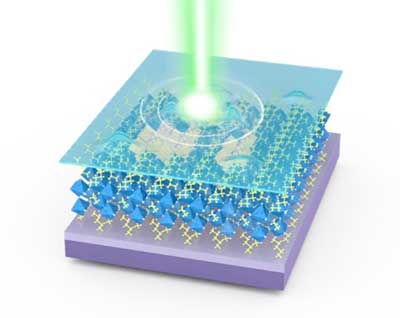 |
| An artist’s impression of laser interaction with a molecularly thin 2D perovskites encapsulated by hexagonal boron nitride (blue layer). (Image: NUS) |
| Layered perovskites are solution processible, low-cost materials that can be used as photo detectors or light emitters. The superior ability of the perovskite crystal to detect and emit light with high efficiency is expected to find practical applications in various fields. Each basic unit of a 2D hybrid perovskite is constructed using a semiconducting layer of inorganic material sandwiched between two organic insulating layers. |
| While researchers have studied layered perovskites in their bulk form for the past thirty years, the properties of these crystals when their thickness is thinned down to a few and single layers have largely not been explored. |
| A research team led by Prof Loh Kian Ping, from the Department of Chemistry, NUS has discovered that a molecularly thin layer of perovskite can be strained in a highly reversible manner without introducing permanent defects on the material that can affect its light emission properties. Also, the emission properties of the perovskite can be tuned reversibly under repeated strains. |
| The researchers achieved this by encapsulating the surface of the perovskite with a thin layer of optically transparent hexagonal boron nitride. This barrier layer traps the organic molecules on the surface of the perovskite layer, preventing them from escaping into the air even under strong laser irradiation. |
| Using a temperature controlled crystallisation method, the researchers synthesised centimetre-sized perovskite single crystals of the Ruddlesden-Popper phase (a form of layered perovskite structure). These specially prepared crystals are much larger than the usual micron-sized ones and allowed the team to peel off thin layers from it using the “scotch tape” method (similar method used for obtaining graphene from graphite). These ultrathin crystals were then used for the experiments. |
| Prof Loh said, “Unlike bulk perovskites where the organic chains of adjacent layers are interdigitated and tightly-packed, the layer of organic chain on ultrathin perovskites can “relax” more easily under laser or thermal activation. This “relaxation” process changes their light emission properties. We found that the light emission can reverse back to its initial state by constraining (“de-relaxing”) the surface of the ultrathin perovskite layer.” |
| “We have also studied the atomic structure of these perovskites using the QPlus atomic force microscope. Depending on the supplied thermal energy, the organic layers on the surface can assemble and change the optoelectronic properties of the crystal in a reversible manner. This could potential be used for developing strain-tuneable optoelectronic devices,” added Prof Loh. |
| Source: National University of Singapore |
|
Subscribe to a free copy of one of our daily Nanowerk Newsletter Email Digests with a compilation of all of the day's news. |

