| Dec 20, 2018 |
Creating nanoscale patterns at record resolution: An instructional video(Nanowerk News) Last year, scientists at the Center for Functional Nanomaterials (CFN)—a U.S. Department of Energy (DOE) Office of Science User Facility at Brookhaven National Laboratory—developed a technique for patterning materials with individual features as small as a single nanometer (nm). |
| When the feature size of materials is reduced from the macroscale to the nanoscale, quantum mechanical effects dramatically alter the materials’ optical, electrical, and thermal properties, enabling new scientific discoveries and future technological applications. |
| Before the development of this technique, patterning materials in a controllable and efficient way at this resolution was not possible. The conventional nanopatterning method of electron-beam lithography (EBL) can typically only resolve features between 10 and 20 nanometers. |
| The CFN scientists pushed the resolution limits of EBL by installing a pattern generator—an electronic system that precisely moves the electron beam over a sample to draw patterns designed with computer software—in an aberration-corrected scanning transmission electron microscope (AC-STEM). |
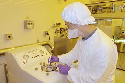 |
| The Journal of Visualized Experiments recently published a video providing step-by-step instructions for a high-resolution nanopatterning technique developed by scientists at Brookhaven Lab's Center for Functional Nanomaterials. |
| The AC-STEM at the CFN is a highly optimized instrument for material characterization at atomic length scales. This optimization enables the routine patterning of lithographic features with record-breaking single-nanometer resolution. |
| Recently, the Journal of Visualized Experiments (JoVE), a peer-reviewed journal that publishes experimental methods in video format, published an of their first-of-its-kind nanoscience tool ("Single-Digit Nanometer Electron-Beam Lithography with an Aberration-Corrected Scanning Transmission Electron Microscope"). |
| In this video, CFN scientists describe a step-by-step protocol to pattern arbitrary structures with single-digit nanometer resolution using the conventional electron-beam resists poly(methyl methacrylate) (PMMA) and hydrogen silsesquioxane (HSQ). |
| The results of their initial work with PMMA, published in 2017 in Nano Letters ("Aberration-Corrected Electron Beam Lithography at the One Nanometer Length Scale"), and the novel results on silicon patterning shown in this video demonstrate how such patterned resists can be used as stencils for transferring nanometer-scale features to metallic and semiconducting materials. |
| “The technique enables the fabrication and study of devices with user-defined nanoscale geometry designed to exploit quantum mechanical effects for fundamental research and potential applications,” said Fernando Camino, a physicist in the CFN Electron Microscopy Group who co-developed the technique. “Currently, we are using the technique to study phase-coherent phenomena in sub-10 nm nanostructures in collaboration with Xu Du of the Department of Physics and Astronomy at Stony Brook University.” |
| Source: Brookhaven National Laboratory |
|
Subscribe to a free copy of one of our daily Nanowerk Newsletter Email Digests with a compilation of all of the day's news. |

